

-
Printed circuit boards (PCBs) are some of the most important components used in electronics, yet they tend to be the most misunderstood. Every PCB must pass through a meticulous design process to ensure that the design is manufacturable at scale, reliable, and has optimal cost. Contrary to other engineering disciplines, PCB design is highly linear and moves through the workflow outlined below.
-
Before you make the leap into designing your own PCBs, make sure you understand the end-to-end PCB design process. Ultimately, this process culminates in a product that can be produced at the required volume with high reliability and operational lifetime. We’ll outline this process and help you understand what to expect from your PCB design services firm.


01
Front-End Engineering & Schematic Capture

_edited.jpg)
Before a designer starts creating a CAD drawing for a PCB, the electrical design and engineering of the product must be completed. Electronics engineers must create their circuits, select important components, and ensure parts can be procured at the required volume. In some cases, simulations are required to better understand circuit functionality and once schematic capture is completed, the engineer will have created a complete database that defines the entire front-end engineering for the product:
-
Schematics in your CAD application’s native file format
-
A preliminary bill of materials (BOM) with sourcing information
-
A complete engineering requirements document for the product
-
A CAD library for components that will be used in the PCB layout
PCB design is performed in electrical CAD (ECAD) applications, and all physical layout data created in ECAD applications are based on the front-end design from the schematic capture tool. The components and circuitry defined in schematic capture will form the basis for the PCB layout, and once completed, a design engineer can move to the next phase of the PCB design process.

02
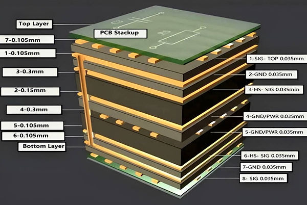
PCB Stackup Design

To ensure the completed PCB is manufacturable at scale, complies with manufacturer’s processing capabilities, and requires minimal design iterations, PCB designers must select appropriate materials for their products. Stackup design centers around material selection and assignment of layer types within the PCB. In some PCBs, correct functionality of the end product will not be achieved unless the right materials are used in the PCB stackup.
PCB designers should contact their manufacturing partner for materials availability and processing limitations before selecting materials and assigning layer functions in the PCB stackup. The goal is to create a stack up that supports the technology being used in the design. RF/microwave PCBs, high-density interconnect (HDI) PCBs, metal-core PCBs, and advanced FR4 PCBs use different classes of materials and require different design approaches in the PCB layout and routing phase.
With a correctly designed stackup, the layout and routing portion will be much easier with fewer iterations required to complete the project. Important performance factors such as electromagnetic interference (EMI), signal integrity (SI), and power integrity (PI) are also related to PCB stackup design, and most of the simple problems in these areas are solved with appropriate layer assignments.
.jpg)

03
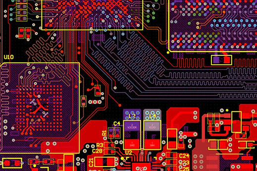
PCB Layout and Routing

.jpg)
The PCB layout is a specific type of CAD drawing that shows the placement of components and copper connections in a PCB. It shows other information as well, such as mask openings, component package outlines, silk screen legend, and the board outline. Following front-end engineering and stackup design, the PCB designer can start creating the PCB layout in their ECAD software. The main tasks include:
-
Complete initial placement based on mechanical constraints and DFM constraints
-
After mechanical back-checking, complete component placement
-
Designing transmission lines based on the PCB stackup design and layer assignments
-
Routing traces and rails on assigned layers
-
Final review and design rule check (DRC) to identify constraint violations
Most of the important SI, PI, and EMI problems that could compromise a product’s functionality and compliance will arise during this phase. An experienced design engineer with correct configuration of design rules will be able to spot these problems before they lead to a field failure. For these reasons, a thorough PCB design review is necessary to ensure any remaining problems are identified and corrected before manufacturing.

04
Design Review and Signoff

A design review is intended to address any remaining problems that might exist in the schematics or PCB layout prior to generating manufacturing data. This involves manual review by an experienced engineer in order to have a 2nd set of eyes on the design. In some advanced products, electromagnetics simulations will be necessary as part of design verification before final signoff. Design review is a group effort and requires checking multiple aspects of the design before signoff for production:
-
Are the manufacturer’s DFM constraints satisfied?
-
Has the BOM been scrubbed of out-of-stock parts?
-
Have all parts/circuits made their way into the layout?
-
Are any leftover DRC errors waived or solved?
-
Has the design been routed based on correct layer assignments?
These are just a few of the aspects that should be examined in a thorough PCB design review. Once the design review is completed and the design has received signoff, manufacturing files are ready to be generated and reviewed before production
.jpg)

05
PCB Manufacturing File Generation

.jpg)
The last mile of PCB design is the generation of the fabrication and assembly outputs required to manufacture the PCBA. These files are in specific formats, which are generated automatically by PCB design software. Once generated, these should be reviewed by the design team and by the manufacturer’s CAM department to ensure they match the CAD data in the PCB layout. Simple configuration settings can create deviations between design and production data, thus a final manufacturing review will be required.
Once the manufacturing files are generated and have passed review, a complete database for the product will be completed and ready to produce at the required volume. The design can then be taken to a manufacturer and put through their standard quoting process.


