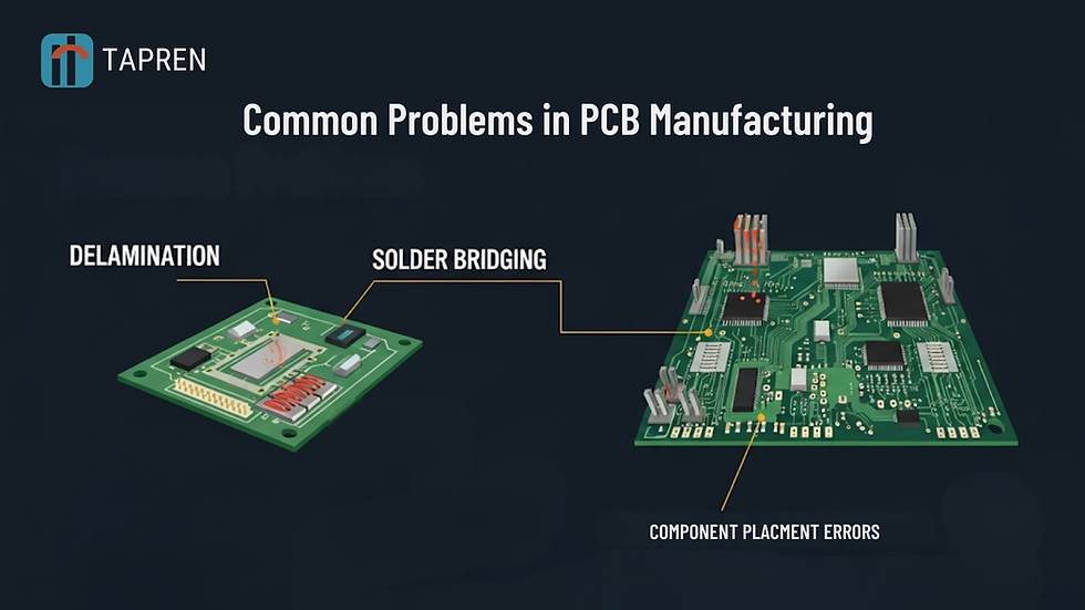
Common Problems in Manufacturing - Part 2
- TapRen Team

- Apr 22
- 6 min read

Abstract
Whether it's tin-spraying issues, solder-mask misalignments, or faulty lamination, these hidden flaws can lead to costly failures and unreliable performance. What if you could spot and prevent them before they cause trouble? In this guide, you'll uncover the most common manufacturing pitfalls and learn simple, effective ways to overcome them, helping you build high-performance, long-lasting PCBs with confidence and precision.
Tin Spraying (HASL) Defects

Tin spraying, also known as Hot Air Solder Leveling (HASL), is a widely used PCB surface finish, but it can introduce several defects that impact board reliability and assembly quality.
What is a HASL defect?
A HASL defect refers to any flaw or imperfection arising from the hot air solder leveling process, such as uneven solder coating, solder bridging, or poor wetting. These defects can cause unreliable solder joints, component misalignment, or even short circuits, especially in fine-pitch or high-density PCB designs
Purpose of Tin Spraying
Tin spraying, also known as HASL, is used in PCB manufacturing to coat copper pads with solder. It helps protect the board and improve solderability.
● Protects exposed copper from oxidation and corrosion.
● Provides a solderable surface for easier component mounting.
● Extends the shelf life of the PCB before assembly.
● Ensures good electrical contact during soldering.
Common Problems in Legend Printing
Legend printing is essential for PCB identification and assembly. However, common printing issues can lead to unclear markings, mislabeling, or missing component information.
● Text gets smudged or blurry, making it hard to read.
● Printed labels don’t line up with the correct components.
● Some markings are missing or not printed at all.
● Letters are too small or unclear to be useful.
Causes and Solutions
Common legend printing problems arise from design and process issues. Identifying their causes helps apply the right solutions to ensure clear, accurate markings on PCBs.
Problem | Cause | Solution |
Smudged or blurry text | Excess ink or an unclean PCB surface | Control ink flow and clean the board before printing |
Misaligned labels | Movement during printing or a wrong setup | Calibrate the equipment and secure the PCB properly |
Missing markings | Errors in design files or printing skips | Check design files and maintain the printer regularly |
The text is too small or unclear | Fonts are too small or low-resolution. | Use recommended font sizes and high-resolution printing |
Solder Mask Defects
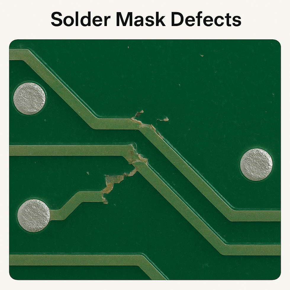
Solder mask defects are critical concerns in PCB manufacturing, as they can compromise both functionality and reliability. Imperfections such as misalignments, pinholes, or insufficient coverage expose copper traces to potential damage, leading to issues like corrosion, short circuits, or signal interference. Identifying and preventing these defects is essential to ensure high-quality, long-lasting circuit boards.
What is the Solder Mask?
The solder mask is the green (or sometimes red, blue, or black) layer you see on a PCB. It covers the copper traces and protects them from oxidation, dust, and accidental solder bridging during assembly. It also helps identify components and improve the board’s durability.
Common Solder Mask Defects
The solder mask protects copper traces from damage, oxidation, and solder bridging. However, defects during application can affect PCB quality, reliability, and overall performance in critical applications.

Misalignment of Solder Mask
Misalignment occurs when the solder mask doesn’t align perfectly with copper pads or traces. This can block pads, cause soldering issues, and lead to short circuits. Proper registration and precise imaging are essential to prevent this manufacturing defect.
Solder Mask Peeling or Delamination
This occurs when the solder mask layer lifts or separates from the PCB surface. It’s usually caused by poor surface cleaning or incorrect curing. Peeling exposes copper traces to air, leading to corrosion and decreased PCB durability.
Air Bubbles and Pinholes
Tiny bubbles or pinholes can form in the solder mask during curing. These defects weaken protection, allowing moisture or contaminants to reach the copper. High-quality materials and careful application help prevent air entrapment during the process.
Solder Mask on Pads
Sometimes, the mask unintentionally covers pads that need to be exposed. This prevents proper soldering and may lead to open circuits. Accurate imaging and careful inspection help avoid this issue and ensure all solderable areas are clear.
Solutions
Preventing solder mask defects requires strict process control, quality equipment, and expert handling to ensure reliable performance and long-term durability of the PCB.
● Use precise printing and alignment machines.
● Maintain a clean and dust-free manufacturing environment.
● Follow proper curing and drying procedures.
● Inspect using AOI (Automated Optical Inspection) to detect early issues.
● Work with experienced PCB manufacturers.
Impact on PCB Reliability
Lamination defects can seriously impact the structure and function of a PCB. These issues often weaken the board, reduce reliability, and may lead to electrical failure over time.
● Delamination can break connections between PCB layers.
● Air pockets weaken the board and affect performance.
● Misalignment can cause signal loss or interference.
● Poor bonding makes the board prone to cracking.
● Resin gaps allow moisture, leading to corrosion.
Defects during PCB Lamination

During PCB lamination, precise control is essential. Any mistakes, such as incorrect pressure, contamination, or moisture, can lead to serious defects that weaken the board and reduce its reliability and performance.
● Improper temperature or pressure during lamination can cause poor bonding between layers.
● Contaminated or dusty inner layers may lead to weak adhesion and delamination.
● Incorrect alignment during stacking can shift layers and damage circuit paths.
● Inadequate resin flow may result in gaps, reducing the board's mechanical strength.
● Moisture trapped in materials can cause blistering or warping during the lamination process.
What is PCB Lamination?
PCB lamination is the process of bonding multiple layers of a printed circuit board using heat, pressure, and adhesive materials. This creates a single, solid board structure. It’s essential for multi-layer PCBs, ensuring electrical insulation between layers and maintaining mechanical strength and stability during use.
Common Lamination Defects
Lamination defects in PCBs can arise from issues during heat and pressure bonding. These faults compromise structural integrity, affect performance, and increase the risk of failure in demanding environments.
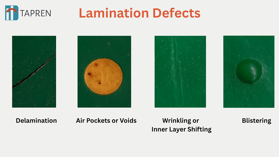
Delamination
Delamination occurs when PCB layers separate due to poor bonding, excessive heat, or contamination. It weakens the structure, affects signal paths, and can lead to circuit failure. Proper pressure, clean surfaces, and correct lamination temperature help prevent this issue.
Air Pockets or Voids
Voids are trapped air bubbles between layers during lamination. These reduce mechanical strength, create uneven surfaces, and allow moisture to enter the board. Using vacuum lamination and clean materials reduces the chances of air entrapment during the process.
Wrinkling or Inner Layer Shifting
This defect happens when inner layers shift or wrinkle during lamination, often due to misalignment or handling errors. It can break trace connections or cause electrical shorts. Careful positioning and pre-bonding procedures help avoid this issue.
Blistering
Blistering is the formation of raised, bubble-like areas on the PCB surface due to trapped moisture or poor curing. These blisters compromise surface quality and reduce electrical performance. Pre-baking materials and controlling humidity help prevent blistering.
Impact on Performance and Reliability
PCB lamination joins all layers under heat and pressure. Mistakes during this step can cause defects that impact strength and reliability.
Delamination can separate layers, causing circuit failure or weak connections.
Voids weaken the board and affect thermal or electrical performance.
Wrinkled or misaligned layers may cause signal loss or interference.
Poor lamination lowers strength, increasing the risk of cracking.
Resin gaps let moisture in, causing corrosion and reliability issues.
Preventing and Overcoming These Problems
PCB manufacturing involves multiple critical steps where defects can occur, such as tin spraying, solder mask application, and lamination. Identifying issues early and applying preventive measures and solutions ensures high-quality, reliable boards.

Conclusion
PCB defects may seem minor, but they can cause major failures in today’s complex electronics. From tin-spraying issues to solder-mask and lamination faults, even small errors can degrade performance and reliability. Understanding these problems sparks awareness and highlights why prevention matters. If you want high-quality, long-lasting PCBs, you need proven solutions and skilled manufacturing. Read on to learn how to avoid these costly issues and ensure your boards meet the highest standards every single time.
FAQs
1. Are all defects visible to the naked eye?
No, many PCB defects, such as internal delamination, microscopic voids, or trace fractures, are not visible to the naked eye. These often require advanced inspection methods such as Automated Optical Inspection (AOI), X-ray inspection, or electrical testing to detect and prevent failures during or after assembly.
2. What are the most cost-effective strategies for reducing PCB defects?
Using Design for Manufacturability (DFM) guidelines, automating inspection, maintaining clean environments, and training staff are cost-effective ways to reduce defects. Early defect detection and process control help avoid rework, material waste, and delays, which significantly lowers overall production costs.
3. How is artificial intelligence being used in PCB defect detection?
Artificial intelligence is used to analyze large volumes of inspection data, detect defect patterns, and identify anomalies with higher accuracy than traditional methods. AI-powered vision systems also reduce false positives and improve decision-making speed, helping manufacturers maintain consistent quality and reduce manual inspection time.
4. How do environmental regulations affect PCB manufacturing defect rates?
Environmental regulations, such as restrictions on hazardous chemicals (RoHS) or emissions control, can influence material choices and process parameters. While these standards improve sustainability, they also require manufacturers to adapt carefully to avoid new defect risks introduced by alternative, eco-friendly materials or methods.


Comments