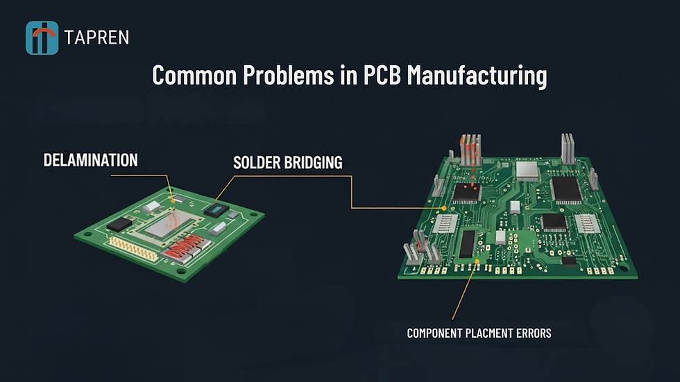
Common Problems in PCB Manufacturing - Part 1
- TapRen Team

- Apr 15
- 7 min read
Updated: Apr 22
Abstract
Do you feel constant frustration due to PCB failure? Even a small fault in a PCB can result in a loss of credibility and a quality issue. Envision your products consistently performing at their peak, without any undetectable flaws. In this blog, you'll find out the most frequent issues in PCB production and implement actionable solutions to make your boards trustworthy and high-quality. Don't allow even the smallest imperfections to derail your success. To find out what will set your electronics apart from the competition, continue reading.
Why is Quality Control Necessary in PCB Production?

Quality control is crucial during PCB manufacturing to ensure every board operates as intended and conforms to design requirements. It identifies and removes defects such as solder joints, open circuits, and short circuits prior to assembly or delivery to customers. The quality checks are primarily conducted through multiple layers of testing to ensure minimal faults in the PCBs. The major problems that frequently occur in PCB manufacturing are electrical testing problems, panelization problems, design-related Problems, manufacturing and yield problems, and finally, process and design problems.
Here, all these problems are discussed, and the ways to minimize them are also provided.
1. Electrical testing
Electrical testing ensures that a PCB operates properly by detecting open circuits, shorts, and incorrect resistance measurements. It confirms that all electrical connections are correct and reliable prior to assembly. This is significant because it detects hidden defects that would otherwise go unnoticed, thereby preventing operational failures. Finally, testing ensures the board is functioning within performance specifications.
Impact of Electrical Testing on Quality and Reliability
Early identification of faults during testing has a positive impact on the quality and reliability of PCBs. Inefficient testing may cause manufacturers to produce large batches of faulty PCB boards, leading to failures and costly repairs. Effective testing ensures that products are in excellent working condition and last longer, creating confidence in customers.
Types of Electrical Testing in PCBs
Electrical testing is a crucial step in the manufacture of PCBs, confirming whether the circuit is in a functional state or not by detecting shorts, opens, and other electrical faults.

1. In-Circuit Testing (ICT)
ICT testing is used in circuit testing to examine every part and connection on the PCB. It is fast and repeatable for large-scale production, but it requires special fixtures and setup time.
2. Flying Probe Testing
Flying Probe Testing utilizes traveling probes to access test points without the need for a custom fixture. This testing is suitable for PCBs with low run volumes and prototypes. It also offers flexibility and lower cost, but it works more slowly than ICT.
3. Functional Testing
Functional Testing confirms the overall functionality of the PCB by performing tests under actual working circumstances. It also confirms that the board operates as intended when powered and fully assembled. Functional testing also identifies faults that the ICT or flying probe tests are unable to detect.
4. Continuity and Resistance Testing
This test verifies that currents flow properly through circuits and that resistance levels are within design specifications. It is employed to detect opens, shorts, and changes that can affect board performance or safety.
Electrical Testing Problems
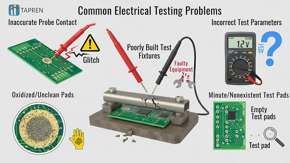
Electrical testing is a crucial aspect of PCB manufacturing, ensuring the adequate connection of all circuits on the board and preventing faults such as open circuits or shorts. Electrical continuity testing before assembly helps producers identify concealed defects in advance, avoid costly failures, and deliver high-quality products.
Common Problems
● Inaccurate results or spurious defects may be caused by probes that improperly touch the test points.
● Pads that are oxidized or unclean may disrupt testing and may lead to failures.
● Poorly built test fixtures may cause damage to the board or fail to test all the necessary points.
● Even after testing, errors in circuit measurement mostly go unnoticed if the test parameters are off.
● Effective test execution may be hindered by minute or nonexistent test pads in the design.
2. Panelization Problems
Panelization is based on the single-board concept, bundling numerous PCBs into a single large board to improve manufacturing productivity. However, the process can also result in spacing alignment problems and separation damage. These factors impact the general quality and yield of the PCB.
What is Panelization?
Panelization is a technique that involves assembling numerous PCBs into a single large PCB, making PCB manufacturing and assembly easier. Instead of inspecting individually, it improves testing efficiency.

Common Methods of Panelization
Panelization involves combining several PCBs into a single panel for simplified manufacturing. Some of the widely used techniques are briefly discussed below.

1. V-scoring
V-scoring produces shallow grooves on the two sides of the panel between the PCBs. The grooves enable easy separation of the boards after production, offering a fast and clean technique that does not harm the boards.
2. Tab-routing with Breakaway Tabs
Tab routing utilizes small tabs to connect separate PCBs within a panel. The tabs retain the boards together during assembly and can be snapped or routed out afterward, providing strong support with simple separation.
3. Mouse Bites
These are perforations in the edges of the PCB within a panel. They allow for easier board separation by breaking along these small connections without stressing or damaging the PCB edges.
3. Design-Related Problems
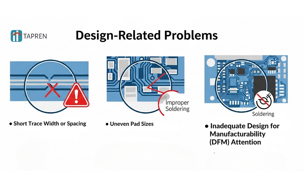
● These problems may arise due to short trace width or spacing, which may lead to open circuits.
● Because of improper soldering, uneven pad sizes are frequently observed.
● Inadequate design for manufacturability (DFM) attention leads to manufacturing problems or higher defect rates.
4. Manufacturing Problems
Manufacturing and yield problems occur when issues during PCB manufacturing result in some boards failing or becoming damaged. This results in material waste and increased costs. The number of successfully manufactured boards can be decreased by flaws such as poor panel design, incorrect spacing, or damage sustained during separation, which can impact manufacturers' overall productivity and profitability.
Legend (Silkscreen) Print Issues
The legend of a PCB is the printed symbols and text that assist in part identification and offer critical information for assembly and fault finding.
What is a legend?
A legend is essentially a printed layer etched onto a PCB to display important information, such as symbols, component marks, and other logos. It assists in assembly and maintenance by helping to locate the parts easily on the board.
Legend Printing Methods
Legend printing labels PCBs with text and symbols for identification. With differing levels of accuracy and detail, popular methods include laser marking, inkjet printing, and screen printing.

Screen Printing
Screen printing employs a stencil and a mesh screen to transfer ink onto the surface of the PCB. It is inexpensive for large numbers but may not be very precise for highly detailed text or intricate designs.
Inkjet Printing
Inkjet printing prints ink directly onto the PCB stencils-free. It is highly precise and well-suited for detailed or small markings and typically used in low- to medium-volume production.
Laser Marking
Marking the PCB surface with a sharp, intense laser beam is called laser marking. While it is particularly suited for traceability and produces lasting, high-resolution marks, it may be more costly than other techniques.
Typical Laser Printing Defects
Legend printing may encounter some common manufacturing issues. The flaws impair readability and may lead to misinterpretation or errors during PCB assembly and testing.

Process & Design Problems
Design and process failures can compromise the performance, reliability, and manufacturability of PCBs. By understanding these issues, the transition from design to production is simplified for manufacturing PCBs.
Common Design Traps
● Using incorrect or unverified component footprints can lead to assembly errors.
● Components that are too close to each other may result in solder bridging or rework issues.
● A smaller trace width or spacing raises the chance of shorts and overheating.
● Inadequate grounding and power distribution may lead to noise and voltage drop.
● Silkscreen overlap with pads may hamper component placement and soldering.

Process Pitfalls
● Delivery of incomplete or flawed design files may cause the manufacturing process to be suspended or delayed.
● Disregarding DFM (Design for Manufacturability) recommendations tends to increase defect levels and production costs.
● Poor solder mask design can lead to solder bridging and expose copper to corrosion.
● Failure to accurately define via and drill sizes can lead to open circuits or manufacturing failures.
● Lack of effective thermal regulation can result in PCB failure and board warping.
Minimizing Ways
Preventing PCB problems depends on good design, clean surfaces, and effective process control. Early involvement of manufacturers and the use of DFM principles prevent expensive defects.

Conclusion
Standard problems in PCB manufacturing, such as electrical test faults, panelization issues, and legend print faults, can significantly impact product reliability and performance. Certain methods, such as rigorous quality control, stringent testing, and design optimization, can help mitigate issues during PCB manufacturing. If the PCB production process is monitored, the final PCB product is likely to be of the highest quality. We are a prominent and experienced PCB manufacturer, dedicated to producing high-quality PCBs that meet our customers' specific requirements and standards. Our objective is to provide the customers with high-grade PCBs that are not only long-lasting and reliable but also cost-effective. Connect with us to experience and learn about the techniques we use to provide such high-quality PCBs.
FAQs
What are some of the unique quality standards that are required for medical device PCBs?
Medical-grade PCBs must be biocompatible, long-term, and safe, as approved by ISO 13485. Rigorous testing and production of medical PCBs in a contamination-free environment, along with regulatory approvals from bodies such as the FDA or the EU MDR, are crucial.
What is the best practice for designing a solder mask?
Verify proper pad clearance, prevent mask slivers, and ensure consistent thickness. Additionally, carefully define solder mask openings to avoid bridging and ensure proper color visibility during inspection. Finally, apply solder mask over vias when necessary and always verify the design against fabrication specs for quality and consistency.
How do contemporary PCB manufacturers approach sustainability and waste?
Manufacturers maintain sustainability and minimize waste by adopting lead-free procedures, which include implementing energy-saving technologies, recycling components, and using chemicals that conserve water. Furthermore, disposing of toxic chemicals away from the point of the water source helps minimize waste and maintain sustainability.
What are the procedures adopted by manufacturers in an attempt to reduce the cost of manufacturing PCBs without degrading their quality?
There are several techniques to maintain a high-quality design while reducing the cost of PCB manufacturing. Certain techniques, such as layer count minimization and the use of standard board sizes, facilitate this process. Additionally, maintaining a neat Gerber file without any unwanted features and choosing components wisely can enhance cost-effectiveness.


Comments