PCB Impedance
- TapRen Team

- Nov 18, 2025
- 8 min read
Updated: Dec 4, 2025

Abstract
In high-speed circuits, such as USB, HDMI, and 5G systems, a single impedance mismatch can compromise signal integrity. Controlled impedance is no longer optional; it's critical.
Maintaining effective impedance control in the PCBs through proper design and fabrication helps prevent signal distortion and enhances performance. Proper PCB impedance control also supports reliable signaling, which is one of the reasons modern PCB designs prioritize it.
This guide explains what it is, how it affects PCB design, and guides you in ensuring your boards meet modern standards.
What is PCB Impedance

It is a quantitative measure of the PCB trace circuits that oppose the flow of AC within the circuit. PCB impedance in DC does not encompass both resistive and reactive components, unlike AC. In PCB traces, impedance mostly depends on the trace geometry, reference plane, proximity, and dielectric material properties. In electronics, a controlled PCB is crucial as it regulates the signal within the circuit, enabling high-speed performance.
Importance of Controlled PCB Impedance

Signal Integrity
Signals at high speeds bounce back if the impedance is not controlled. These reflections modify the signal shape, leading to faults such as incorrect data or uneven clock cycles. Maintaining the impedance in a controlled manner along the trace provides a clean signal in a readable form.
Power Delivery
Stable impedance helps to provide clean power throughout the PCB within components. At the same time, unstable impedance leads to sudden voltage spikes, which cause instability. Proper impedance reduces noise and enables the system to operate smoothly, even when power demands fluctuate.
Reducing EMI (Electromagnetic Interference)
EMI is an unwanted noise that can affect signal integrity and cause poor impedance, leading to circuit traces acting as interference or signal antennas. PCB impedance, which is regulated, allows signals to remain on the lane, thereby reducing noise.
Improving System Performance
Impedance control is essential while working with high-frequency signals above 50 MHz. If the signal varies in impedance within the components of the PCB, it results in distortion and slows down the performance. This also leads to errors in high-speed consumer devices, such as routers and servers.
Meeting Industry Standards
Devices like USB, PCIe, and Ethernet require specific impedance differential values such as 50Ω or 90Ω. If the PCB does not meet these industry-standard values, the product may not function properly. Controlled impedance is heavily dependent on design control, which also ensures that the design complies with relevant regulations and standards.
Example of PCB Impedance
Let us consider an example of a high-speed digital interface running at 3.2 GHz between a processor and memory. Components in the PCB are designed to connect them along the trace with a single-ended impedance of 50Ω. On the top layer, the traces are 5 mils wide, with an FR-4 dielectric (εr ≈ 4.2) thickness of 4 mils to the reference plane.
If the impedance is not regulated, there is a high chance that the memory interface will experience data corruption due to signal reflections. Reflections are minimized, and clean signals are allowed to pass through the processor due to controlled impedance.
The processor can then read from and write to memory at reliable speeds. After the design has been fabricated, its impedance is finalized using Time Domain Reflectometry (TDR) testing, which ensures that the actual impedance closely matches the target within a ±10% tolerance.
PCB Impedance Formula
PCB impedance is primarily determined by the trace configuration. These are some of the key formulas for standard trace configurations:
Microstrip (Surface Trace)

For a trace on the outer layer with a reference plane below:
Z₀ = (87 / √(εr + 1.41)) × ln(5.98h / (0.8w + t))
Where:
Z₀ = Characteristic impedance
εr = Dielectric constant of the material
h = Distance between the trace and reference plane
w = Width of the trace
t = Thickness of the trace
Stripline (Internal Trace)

For a trace between two reference planes:
Z₀ = (60 / √εr) × ln(4h / (0.67π × (0.8w + t)))
Where:
h = Two distance sample planes
Other variables are the same as microstrip
Differential Pairs

For two traces carrying differential signals:
Zdiff = 2 × Z₀ × (1 - 0.48e^(-0.96s/h))
Where:
Zdiff = Differential impedance
Z₀ = Single-ended impedance of each trace
s = Spacing between the traces
h = height from a reference plane
These formulas provide a good estimation using simple calculations. Field solver software could be used to calculate the impedance precisely, especially for complex geometries.
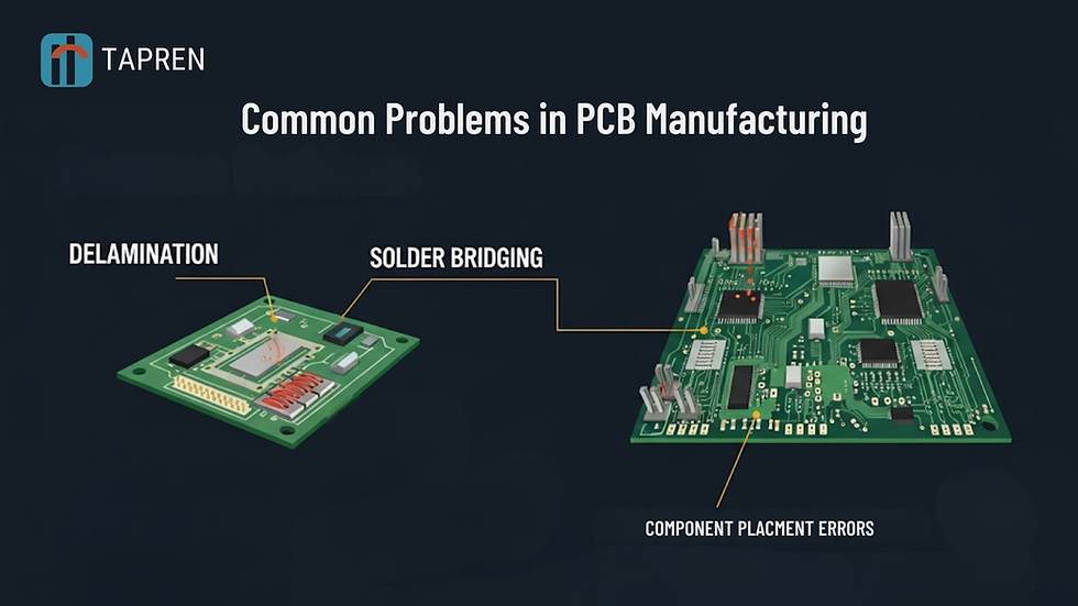
Common Impedance Problems

Various problems may arise in controlled PCB Impedance, some of which are outlined below.
If the PCB trace doesn’t match the load impedance in the source, signals get reflected back, which degrades the signal quality.
Impedance mismatches may also cause signal distortion, which ultimately affects the accuracy and clarity of the data transmission.
Uncontrolled impedance may also result in Excessive electromagnetic interference (EMI), which leads to noise that can disrupt the signaling in nearby circuits.
PCB impedance in the trace might lead to a reduction of performance and bandwidth.
Variations in trace width or dielectric properties, along with manufacturing issues, may cause sudden impedance changes and impact the reliability of the circuit.
Improper designs and reference planes can also lead to impedance discontinuity, which causes problems in signal integrity.
Design Tips to Reduce PCB Impedance

To reduce impedance in a PCB, maintaining a uniform trace width with equal spacing throughout the board is recommended.
For reducing PCB impedance, dielectrics with uniform properties should be used.
The trace should not be bent, as this may result in sharp bends, which can cause impedance discontinuities.
Furthermore, the differential pairs should be designed to have equal spacing and trace length.
Ensure that the reference planes are positioned closer to the signal layers, which helps maintain better impedance control.
How We Measure & Maintain Impedance in Manufacturing

To measure impedance, tools such as Time-Domain Reflectometry (TDR) or Vector Network Analyzers (VNA) are used. The companies first test it on the PCB sections that mimic the impedance of the main board to ensure the actual PCB meets the design’s impedance requirements.
This is done using test coupons, which ensure that the PCB meets the actual impedance necessity. Primarily, maintaining precise trace impedance involves precisely stacking layers made up of specific materials with consistent properties and dimensions.
How to Match Impedance in PCB?

Impedance in PCB could be matched using the following reasons
Based on the signal standards, for example (e.g., 50Ω or 90Ω), the required signal impedance is calculated.
To match the target impedance, trace widths are designed accordingly. Also, spacing and stacking are maintained to achieve the target impedance afterward.
Impedance matching can also be done using various simulation tools or calculators for accuracy, which saves time and effort.
Finally, the impedance can be tested using a time-domain reflectometer (TDR) or vector network analyzer (VNA), and the designs can be adjusted as necessary.
Common PCB Impedance Mistakes & How to Avoid Them

Some of the major mistakes and ways to avoid them are highlighted here.
Neglecting impedance in high-speed designs
The majority of high-speed circuit designs do not precisely manage impedance, which may lead to data errors and signal reflections. Always consider impedance from the outset, especially for high-frequency signals, to maintain signal integrity and ensure reliable device functioning.
Incorrect stack-up or material selection
Incorrect PCB stack-up or use of materials with unknown dielectric constants will result in impedance discrepancies and signal loss. Select stable, well-established materials and carefully design the layer stack to achieve a consistent impedance throughout the board.
Inaccurate trace width or spacing
Straying from designed trace widths or spacings may result in impedance mismatches. Utilize impedance calculators and maintain close manufacturing tolerances to ensure trace sizes meet design specifications and retain signal integrity.
Poor documentation
During PCB manufacturing, failing to specify impedance requirements and stack-up details in the design files can lead to manufacturing errors. When manufacturing PCBs, provide detailed and clear documentation to guide manufacturers in producing boards that meet the impedance control standards.
Why Choose TapRen?

TapRen is a trusted PCB factory that excels in manufacturing high-quality, impedance-controlled boards. With leading tools, expert support, and stable processes, TapRen ensures that your high-speed designs consistently meet quality, performance, and industry standards.
Precision Engineering
TapRen utilizes state-of-the-art design tools and engineering expertise to ensure precise impedance control on every board. Their professional staff maintains precise control over trace geometry and layer stack-up, offering consistent performance even in complex, high-frequency applications and multi-layered PCB designs.
Advanced Testing Tools
To ensure boards of all specifications, TapRen utilizes advanced equipment, including Time Domain Reflectometry (TDR) and network analyzers. The equipment verifies the actual impedance of PCB traces and helps detect discrepancies before they reach the customers.
Customized Stack-Up Support
TapRen collaborates with designers to create custom stack-ups tailored to specific impedance requirements. Whether you need a single-ended 50Ω or 100Ω differential setup, their experts recommend the right materials and trace widths to obtain the particular desired impedance.
Reliable Quality and Fast Shipping
TapRen provides advanced quality controls and efficient production techniques. They ensure each order is precise, reliable, and dispatched on schedule. Whether it's a prototype or mass production, they achieve a quick turnaround without sacrificing quality.
Compliance and certifications
TapRen is certified to international standards such as ISO, RoHS, and UL. These indicate that they are dedicated to quality, safety, and the environment. Choosing TapRen guarantees your boards are built to global compliance standards for most industries.
Case Study 1: Analysis of PCB to Find Trace Impedance by Method of Moments and Cross-talk Interference
This paper utilizes PCB trace impedance and crosstalk interference using the Method of Moments (MoM). Capacitance, along with inductance, is calculated for crosstalk approximations in various situations. Experiment values used for verification are compared with MATLAB simulations and HFSS modeling using a network analyzer. The argument guaranteed accuracy. This study focuses on the trace geometry design and electromagnetic coupling in PCB designs intended for high-speed applications. It also provides various techniques for analyzing impedance and crosstalk reduction in a microstrip arrangement.
Case Study 2: Statistical Estimation of Characteristic Impedance Distribution Caused by PCB Manufacturing Process Variation in High-Speed Mobile Channels
A statistical method of predicting characteristic impedance distribution in high-speed mobile PCBs under the influence of manufacturing variation is discussed in this article. With thinner PCBs, the design becomes more susceptible, and traditional design rules cannot prevent signal quality degradation. The technique utilizes probability density functions of the PCB parameters to model impedance variation, introducing a "noteworthy range" to quantify design strength. Tested on two-channel designs, the technique found one with 24% reduced variation and lower timing jitter, which certified its usefulness in pre-design screening to improve immunity to process defects.
Key Takeaways
Impedance control is vital in high-speed designs.
Choosing the appropriate PCB material and stacking it with a consistent width is essential.
Effective communication with the manufacturers improves results.
Comprehensive testing can further validate the design requirements.
Proper documentation ensures that manufacturing can be carried out further.
FAQs
Why is 50-ohm impedance so common in electronics?
50Ω came as the optimal compromise between power capability and signal attenuation in coaxial cables. It was the de facto standard for test equipment, including radio frequency and high-speed models. The majority of receivers and drivers are optimized for 50Ω systems.
What is the cost difference of a standard PCB when compared to a controlled impedance PCB?
Controlled impedance increases the cost of PCB by 15-30% due to the use of special materials, tighter manufacturing tolerances, and additional testing. However, it prevents expensive system failures and redesigns and is cost-effective for high-speed systems.
How do I know if my design needs impedance control?
If your signal rise time is less than 2× the trace propagation delay, you need impedance control. Rule of thumb: Clock speeds greater than 50 MHz, data speeds greater than 100 Mbps, or any high-speed interface (such as USB, HDMI, PCIe, or DDR) require controlled impedance.
Do I have to simulate impedance before PCB production?
Yes. Altium Designer, Polar SI9000, or HyperLynx software allows for impedance simulation. They allow you to make changes to trace width, trace spacing, and material selection to meet the target impedance before you finalize the design.
Is impedance tunable after the PCB is already constructed?
No, once PCB is manufactured, impedance cannot be defined. It is a function of trace width, trace spacing, and layer stack-up, which are described in the production process. To ensure proper impedance, the PCB must be designed appropriately and calculated before manufacturing.


Comments