Why Are Six-Layer PCBs Widely Used?
- TapRen Team

- Sep 7, 2025
- 7 min read
Updated: Nov 3, 2025

Abstract
As the compactness and power of electronics increase, effective, efficient, and high-performance PCB designs with rising demands are becoming necessary; however, with numerous multilayer PCB types available, 6-layer PCBs have emerged as the top choice among engineers due to their superior performance, space efficiency, and cost-effectiveness. 6-layer PCBs provide enhanced signal integrity, improved EMI control, and optimized power distribution, making them ideal for high-speed and complex applications. Whether in consumer products, industrial machinery, or IoT applications, six-layer PCBs provide the flexibility and reliability needed to meet today's design requirements without the added expense of higher-layer configurations. This article explores the benefits of six-layer PCBs, their applications, and how they compare to 4- and 8-layer designs.
What is 6 Layer PCB?

A 6-layer PCB features six layers of copper traces stacked on top of each other, separated by insulating material. They typically include:
Two outer signal layers (top and bottom)
They are generally utilized for routing high-speed or critical signals and components. Because they are on the outside, they are easily accessible for soldering and testing.
Two internal signal layers
These provide a larger routing area for intricate designs with improved differentiation of signal types and reduced crosstalk between tracks.
Two or more plane layers (commonly ground and power, but can include multiple ground planes depending on EMI requirements)
These solid copper ground planes, strategically placed between signal layers, provide clean return paths and shielding to reduce electromagnetic interference (EMI). Two single-purpose ground planes are used rather than one in some constructions, especially those involving high-speed or sensitive analog-digital mixed designs, to attenuate EMI further and improve signal integrity. The positioning and selection of these planes are determined by the stackup strategy and the electromagnetic compatibility (EMC) requirement of the circuit.
When to USE 6-LAYER PCB?
6-layer PCBs are suitable when:
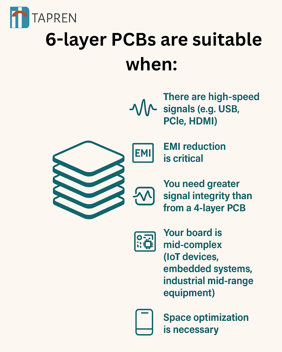
There are high-speed signals (e.g., USB, PCIe, HDMI)
High-speed signals require controlled impedance and clearly defined return paths to maintain signal integrity. With a 6-layer stackup, such signals can be routed with little crosstalk and distortion.
EMI reduction is critical
Electromagnetic Interference penetrates sensitive electronics and is an issue in meeting standards. Isolated power and ground planes in a 6-layer PCB provide shielding, deradiation, and noise minimization.
You need greater signal integrity than is possible from a 4-layer PCB
Since additional routes and planes are available, a 6-layer PCB minimizes reflections, decreases delay, and reduces interference. The outcome is a purer transmission of signals on the board.
Your board is mid-complex (IoT devices, embedded systems, industrial mid-range equipment)
When your layout has a combination of analog, digital, and power signals, a 6-layer board is sufficient to isolate them from one another and trace them neatly. It's suitable for moderately complex designs and is cheaper than adding extra layers.
Space optimization is necessary
As board sizes decrease, increased functionality must be accommodated in smaller form factors. A 6-layer board supplies tighter routing densities and smaller form factor designs, which are ideal for handheld and space-constrained applications.
6 Layer PCB Stackup

There are four widely used 6-layer PCB stackup configurations. The choice depends on design priorities such as EMC performance, signal integrity, power distribution, and routing complexity. Below are the four most common stackups, with a brief explanation of each layer’s role.
Signal – Ground – Signal – Signal – Ground – Signal
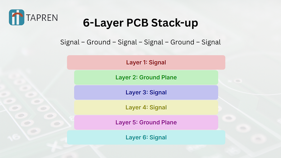
This configuration provides excellent EMI performance and signal integrity by sandwiching the inner signal layers between two ground planes. All signal layers are adjacent to a solid reference plane, which ensures low-impedance return paths and minimal noise.
Signal – Ground – Signal – Power – Ground – Signal

This stackup provides a balanced approach to both power integrity and EMI control. The ground planes on Layers 2 and 5 serve as return paths for signals and also provide isolation between power and signal planes.
Signal – Ground – Power – Power – Ground – Signal

This setup is designed for systems requiring multiple power rails. It places dual power planes between two ground planes, isolating power domains and maintaining clean references.
Signal – Power – Ground – Ground – Power – Signal

This stackup is typically used when the design has very strict EMI or power noise constraints. It provides a symmetric structure with tightly coupled power-ground pairs for decoupling and multiple ground layers for shielding.
Design Considerations of Six-Layer PCB

Thorough planning is essential for designing a 6-layer PCB to achieve optimal electrical performance, manufacturability, and reliability. The additional layers create more freedom, but good routing, impedance, and power distribution planning must be used to their full potential.
Follow these important considerations every engineer needs to remember:
Impedance Matching for High-Speed Signals
High-speed signal integrity requires consistent impedance. Designers must use proper trace spacings and widths according to the stack-up to avoid signal reflections and losses.
Signal Return Paths and Reference Planes
Signals require a clean and uninterrupted return path, typically through nearby ground planes. Proper reference plane placement minimizes the loop area, minimizing EMI.
Power Integrity through Decoupling Capacitors and Clean Planes
The stable power supply is ensured by using decoupling capacitors near ICs and providing uninterrupted power planes. This prevents voltage drops and minimizes noise across the board.
Routing Density – Especially for BGA Components
6-layer PCBs offer more space to route challenging packages like BGAs (Ball Grid Arrays). Correct layer allocation leaves space for routing critical signals as best as possible without abusing vias.
Thermal Management – Copper Weight and Via Design
Heat management is essential, especially in power-dense applications. Adequate copper thickness and thermal vias effectively dissipate heat, thereby enhancing the board's reliability.
Where Six-Layer PCBs Are Making an Impact?

Six-layer PCBs are the standard issue across industries that demand a mix of compactness, performance, and reliability. Their versatility also makes them a smart choice for products that demand moderate complexity and high-speed communication without increasing cost and design effort, as with more layered boards.
Here are some of the key industries where 6-layer PCBs are delivering real-world benefits:
Consumer Electronics
Smartphones, tablets, and smartwatches use 6-layer PCBs to accommodate dense routing in a compact area. They offer the EMI control and signal integrity that high-speed interfaces such as USB-C and wireless modules demand.
IoT Devices
IoT devices, from home automation systems to industrial sensors, benefit from 6-layer PCBs due to their compact form factor and layered signal isolation. The extra layers provide support for mixed-signal environments and wireless connectivity, reducing noise interference.
Automotive
Infotainment modules, ADAS, and sensors in modern cars—each of which requires high-speed data communication with high robustness—are protected from EMI and powered by 6-layer PCBs.
Medical Devices
Portable diagnostic equipment and wearable devices utilize 6-layer PCBs to conserve space for signal processing. Accurate power transfer and effective noise management are crucial for obtaining precise measurements and ensuring machine reliability.
Telecommunication
PCBs are needed in routers, switches, and base stations to handle multiple high-speed data lines. Six-layer designs for small network hardware cover signal routing at high frequency, grounding, and thermal management.
Engineering Considerations Before You Stack

Electrical and mechanical factors must be addressed before releasing a 6-layer PCB stackup to ensure that the design's performance is assured. Whatever is applied here directly affects signal integrity, manufacturability, thermal profile, and ultimate reliability.
Have the following important engineering factors in mind to guarantee:
Determine Signal Speed and Bandwidth Requirements
High-speed signals require low impedance and controlled noise. Knowing your design's bandwidth needs enables layer assignment and material selection in the name of signal integrity.
Estimate Layer Utilization and Routing Complexity
Estimate the number of power, signal, and ground traces required per layer. A good 6-layer board provides routing flexibility and EMI control without complicating the layout.
Select Via Types (e.g., Blind, Buried, Through-Hole)
With selection, determine routing density, access to layers, and manufacturing cost. Blind and buried vias are space-efficient but manufacturing risky, while through-hole vias are simpler but require a precious routing area.
Perform Pre-Layout Impedance and EMI Simulations
Impedance and EMI simulation software help identify problems before the layout is finalized. Such software verifies impedance targets, identifies areas of crosstalk, and allows anticipation stack-up adjustments.
Choose the Right Stack-Up Configuration for Thermal and Electrical Performance
The ideal stack-up (i.e., plane location, signal layer ordering) matters depending on your application—high-speed, power-dense, or mixed-signal. A properly engineered stack-up translates to good heat dissipation, lower noise, and acceptable performance.
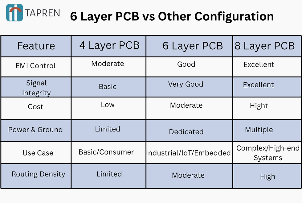
6 Layer PCB vs Other Configurations
Case Study
How does a 6-layer PCB solve EMI Issues in a Medical Scanner?
EMI issues and complex signal routing were encountered by designers when designing a compact medical optical scanner. Elements such as switching regulators, inductors, and a 64-pin LQFP microcontroller posed severe interference hazards, making it complex to create the PCB layout. The switch to a 6-layer PCB proved to be the magic solution.
The team achieved cleaner signal paths and improved thermal management by isolating noisy components, utilizing polygon pours for high-current traces, and minimizing microcontroller breakout routing. However, the dedicated ground and power planes significantly reduced EMI, allowing for stable voltage distribution throughout the board. The increased routing density, facilitated by the additional layers, allowed everything to fit within tight size constraints. This practical application shows how 6-layer PCBs can handle average complexity with better performance, making them a smart investment for today's applications where space, reliability, and signal integrity are most critical.
Key Takeaways
Six-layer PCBs provide manufacturers and design engineers with the optimal balance between technological complexity and cost, while also offering enhanced performance capabilities. EMI control, along with improved signal performance and power distribution, makes these PCBs a reliable method for high-frequency applications with small size requirements. Multiple future-proof applications find value in their flexibility, benefiting IoT and medical device developments. Small, quick, smarter electronic requirements drive manufacturers to choose the time-tested 6-layer stackup design. The 6-layer PCB design represents a perfect compromise between moving up from a 4-layer board and preventing increased expenses associated with an 8-layer design.
Do you need better signal clarity, less noise, and a smarter layout without blowing your budget? Our 6-layer boards offer the perfect balance of performance and reliability, ideal for compact, high-speed designs.
FAQs
Why is heat dissipation important in PCB design?
Heat dissipation is essential, as too much heat can damage components, reduce performance, and shorten the life of a PCB. Satisfactory thermal management will keep the PCB at safe temperatures and avoid failures.
What is the advantage of thermal vias in PCB heat dissipation?
Thermal vias provide a path for heat to travel from one layer of the PCB to another, allowing heat to escape more easily. This technique distributes the heat evenly across the board, ensuring that no hotspot overheats and the board maintains a suitable operating temperature.
Do ventilation and airflow influence heat dissipation from PCBs?
Natural airflow and ventilation around a PCB can significantly contribute to its heat dissipation. Adding cooling fans or vents, or placing the PCB inside an enclosure that provides airflow, can efficiently pull heat away from heat-sensitive components to prevent overheating.


Comments