Zero PCB: Mastering Permanent Prototyping
- TapRen Team

- Jul 16, 2025
- 7 min read
Updated: Aug 27, 2025

Abstract:
Zero PCBs, also referred to as general-purpose PCBs, are a type of prototyping board used in various electronic developments. Unlike standard PCBs, which are designed with copper traces pre-defined, zero PCBs are perforated and allow the user to wire the circuits themselves according to project requirements.
The article presents an in-depth overview of Zero PCB, covering types, materials, features, and their differences in relation to breadboards. Additionally, we have provided a step-by-step explanation of the soldering technique, indicated general applications of the DIY and professional prototypes, and discussed effective use.
What is Zero PCB?
Zero PCB is a prototyping board featuring a grid of evenly spaced holes that enables the manual mounting and interconnection of electronic components. In contrast to pre-etched circuit boards, on a Zero PCB, there is complete freedom in the circuit design. It is useful for experimental and small projects, providing a quick way to test, debug, and refine a circuit before ordering a final PCB layout.
These boards are very popular among hobbyists, students, and professionals for testing circuit concepts before moving on to custom PCBs. Zero PCBs are available in various materials and thicknesses; therefore, they represent an affordable and durable means of creating electronic prototypes.
1. Features of Zero PCB
Zero PCBs are designed to be both flexible and strong enough to produce prototypes or small-scale circuitry. In fact, specific characteristics make it the first choice for building solid and long-lived electronic circuits. The key highlights of Zero PCB are given below:
1.1 Perforated Grid Layout

All Zero PCBs contain a regularly spaced grid of holes, normally at a 2.54mm (0.1-inch) pitch. This standard spacing allows them to support most electronic components, hence making the assembly of a circuit easier.
1.2 Copper-Plated Pads
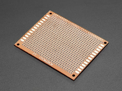
Most of the Zero PCBs are pre-provided with copper pads around the holes. It enhances solderability and electrical connectivity. This helps in sustaining robust and reliable solder joints by reducing the risk of broken connections.
1.3 Durable Base Material

Zero PCBs are manufactured from FR4, a fiberglass-reinforced epoxy material, or FR2 phenolic resin, serving to provide rigidity, resistance to heat, and flexibility for the board in different ways. It means the material chosen will determine how durable and functional it will be.
1.4 Variety in Thickness

Zero PCBs offer different thickness options, mostly between 1.0mm to 2.0mm. Thicker PCBs offer better mechanical stability and heat dissipation, while thin ones save weight and space.
1.5 Customization Capability
Unlike pre-designed PCBs, Zero PCBs can be manually cut, drilled, or shaped to fit the project requirements. This flexibility in the design enables users to create tailored designs that accommodate unique circuit layouts.
2. Types of Zero PCB
Zero PCBs come in many forms, each being developed to cater to different prototyping requirements. A board choice depends on several factors: the complexity of the project, durability, and ease of assembly, among others. Some of the most applied types of Zero PCB are given below.
2.1 Single-Sided Zero PCB

This is the most basic form, having conductive copper pads on only one side of the board. This is suitable for simple circuits that contain fewer components, providing a very easy-to-use platform for beginners in prototyping.
2.2 Double-Sided Zero PCB

Unlike the single-sided one, they feature copper pads on both sides, allowing for more complex circuitry. They have greater design flexibility and, as such, permit better utilization of space. Therefore, they can be used in projects that have a higher component density.
2.3 Pre-Tinned Zero PCB

In such boards, a thin layer of tin coating is applied over the copper pads to enhance solderability and prevent oxidation. A feature like that will make them excellent to use when one needs a good and long-lasting electrical contact.
2.4 Fiber-Based Zero PCB
These boards are typically made from FR4 (fiberglass-reinforced epoxy) or FR2 (phenolic resin) materials, resulting in varying strengths for durability and temperature tolerance. FR4 variants are stronger and can handle high-temperature applications without much issue, whereas FR2 variants are the less expensive options suitable for general prototyping.
Each Zero PCB variant offers some advantages based on the project requirements. A proper board selection ensures better performance, longer lifetime, and easier assemblability of the circuit.
3. Materials Used in Zero PCB

Zero PCBs can be made from various types of materials, each with its unique characteristics that determine durability, heat resistance, and ease of use. Application and environmental factors determine which material is selected. The following are some common materials for manufacturing zero PCB:
3.1 FR4
FR4 is among the most popular material types, boasting excellent strength, heat resistance, and electrical insulation. FR4 comprises fiberglass cloth with a woven structure and an epoxy resin binder.
3.2 FR2
This is the low-budget version of FR4, manufactured using a paper-based composite impregnated with phenolic resin. It lacks the robustness of FR4 in terms of withstanding higher temperatures; however, due to its lightness and affordability, it performs well enough for low-power applications and general-purpose prototyping.
3.3 Copper-Clad Boards
These are made with a thin layer of copper laminated onto the base material. Copper makes the substrate conductive; these require more processes, such as etching or manually adding wire over the surface.
The material selection for Zero PCB is crucial in determining the board's performance, thermal stability, and longevity; therefore, the material must be matched to the application.
4. Zero PCB vs. Breadboard

Zero PCBs and breadboards are both used for prototyping circuits, but they differ in function, strength, and application. Breadboards enable the assembly of temporary circuits without the need for soldering, making them ideal for preliminary tests. However, they can be unreliable because loose connections may occur, particularly with limited current handling. On the other hand, Zero PCBs use soldering to place components, thereby creating permanent joints that are stable and suitable for use over a relatively long period in higher-power applications.

5. How to Solder on Zero PCB
Soldering on a Zero PCB is anything but complicated, opening up a wide field of possibilities for developing personalized electronic circuits. It is, however, essential to learn how to solder on a Zero PCB, whether for hobby purposes or professional use, when developing reliable electronic projects. The following is a review of essential tools, techniques, and tips necessary for effectively soldering on a Zero PCB.
Recommended reading: Manual Soldering Tips and SMT Soldering
5.1 Tools and Materials Needed
Gather the following materials and equipment before you start soldering:
Soldering Iron: A good, fine-tipped soldering iron is needed to do the work on a Zero PCB.
Soldering Iron Stand: To safely hold your soldering iron.
Wire Cutters: To trim excess leads after soldering.
Tweezers: Handy in positioning small components on the Zero PCB.
Safety Glasses: Protect your eyes from damage caused by flying solder.
Flux: Good flow and adherence, though not necessary.
5.2 Preparing the Zero PCB
Cleaning the Board: Ensure your Zero PCB is free from dust and grease. Dip a little isopropyl alcohol onto a lint-free cloth to help clean the surface.
Position the Components: Place the components onto the board according to your circuit design. Use a tweezer to pick up small parts, ensuring they are not misaligned.
Secure Components If necessary, tape down or use a small amount of adhesive to hold components in place while soldering.
5.3 Soldering Steps

Heat the Soldering Iron: Turn on your soldering iron and allow it to reach the appropriate temperature, approximately 350°C to 400°C. A well-heated iron is crucial for good soldering.
Apply Heat to the Joint: Let the soldering iron tip touch the component lead and the Zero PCB pad simultaneously. Let it remain for about 1 second to heat the two surfaces properly.
Feed in Solder: With the soldering iron in place, feed solder into the joint. Allow the solder to flow around the connection, then remove the solder first and the iron afterward to avoid a cold joint.
Inspect the Joint: A good solder joint should be bright, smooth, and cone-shaped. Any cold solder joints with dull, grainy, or poorly adhered connections should be reheated to ensure a strong electrical and mechanical bond.
Trim Excess Leads: Use wire cutters to snip off any extra leads protruding from the soldered joint, making it neat and tidy.
6. Applications of Zero PCB

Zero PCBs are flexible, unpatterned boards used in everything from hobbyist to professional electronics because of their flexible platform for custom circuit design and assembly. This includes:
6.1 DIY Projects

Zero PCBs are among the favorite methods of hobbyists creating custom electronic circuits, allowing experimentation and creativity in projects ranging from simple LED displays to complex microcontroller designs.
6.2 Teaching Tools in Electronics Courses

Zero PCBs are very useful teaching tools in electronics courses. Through practice and experience, students learn how to design circuits and employ various soldering techniques.
6.3 Wearables

Today's increasing trend toward wearables makes Zero PCBs a compact electronic solution for wearable devices.
6.4 Custom Sensors and IoT Devices

Zero PCBs are extremely popular in prototyping for IoT and embedded systems. The speed of design for sensors and controllers enables developers to test concepts for smart devices quickly.
7. Key Takeaways
Zero PCBs are a necessary element in the process of prototyping, providing strength and cost-effectiveness while constructing electronic circuits. While they require soldering skills, their permanence makes them ideal for finalizing designs before transitioning to mass production. Be it for DIY projects or professional prototyping, and Zero PCBs remain a handy tool for both electronics enthusiasts and engineers alike.
TapRen is a top PCB design company at the forefront of innovation. With our expertise in designing and manufacturing advanced PCBs, we're constantly pushing the limits of what's possible in modern electronics. Get in touch with us today to see how we can help you stay ahead in this rapidly changing field!
8. FAQs
Are Zero PCBs reusable?
No, the board cannot be reused once it has been soldered, like a breadboard.
What is the best soldering iron for Zero PCB?
The 15W-30W soldering iron is perfect for most applications.
How can zero PCB be prevented from short circuits?
Utilize insulation techniques, such as heat shrink tubing and proper soldering practices.


Comments