What is PCB Potting? Complete Guide to Compounds, Process & Design Tips
- TapRen Team

- Nov 10, 2025
- 8 min read
Updated: Nov 18, 2025

Abstract
Potting is a routine practice where electronic assemblies are sealed in a protective compound to protect against moisture, dust, vibration, and chemical exposure. The article provides comprehensive coverage of PCB potting, including applicability, components, potting process, design rules, advantages, and disadvantages.
This article covers the standard usage and discusses the latest developments, as well as industry standards, for potting technologies.
What is Potting in PCB?
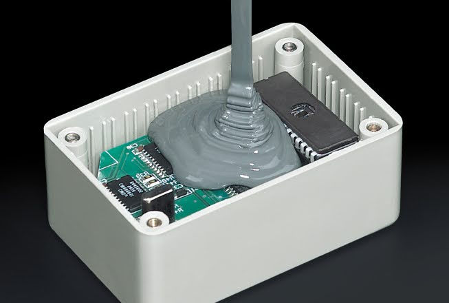
RPCB potting is the process of encapsulating a printed circuit board (PCB) and its components in a protective, gel-like, or solid-insulating material. Common potting compounds include epoxy, silicone, and polyurethane. This material completely surrounds the assembly, forming a sealed barrier against external elements.
Potting protects the electronics from moisture, dust, chemicals, vibrations, and extreme temperatures. It also enhances mechanical strength, provides electrical insulation, and improves resistance to tampering. Once cured, the potted PCB is more durable and capable of withstanding harsh operating environments.
Why Potting Is Crucial for PCBs?
Potting is one of the most crucial aspects in enhancing the reliability and durability of PCBs, particularly when used in harsh or aggressive environments. It encapsulates the board from moisture, dust, chemicals, and physical shocks that could otherwise result in corrosion, short circuits, or mechanical failure.
Potting also provides electrical insulation between elements and helps control thermal stress by distributing heat more uniformly. For highly sensitive or vibration-prone applications, potting helps enhance the mechanical integrity of the assembly. Potting also offers tamper resistance, as it is difficult for unauthorized individuals to penetrate and reverse-engineer the circuit.
Types of Potting Compounds

Selecting the correct potting compound is crucial for providing long-term service and protection to a PCB. The compound must be compatible with the operational environment and performance requirements of the electronic assembly. The three most common compounds used are epoxy, polyurethane, and silicone, each with varying features that make them suitable for specific applications.
Epoxy Compounds
Epoxy is a physically hard-curing material that exhibits high strength, adhesion, and resistance to chemicals and moisture. The complex and strong barrier that epoxy forms over the PCB is utilized in environments exposed to physical stress and harsh conditions. It is very difficult to remove once cured, making it challenging to rework and repair.
Polyurethane Compounds
Polyurethane is softer and more flexible than epoxy, making it better suited for applications that are subject to vibration, shock, or heat expansion. It cures to a less rigid state, reducing stress against delicate components. Less heat-resistant than epoxy, it nevertheless possesses acceptable resistance to water, chemicals, and abrasion by mechanical means.
Silicone Compounds
Silicone is highly flexible and can withstand extreme temperatures; hence, it is the most sought-after material for high-temperature and high-performance applications. Silicone is elastic in the cured form and will not crack when materials expand and contract without damaging anything. Silicone is also simpler to rework than epoxy or polyurethane, and hence it is perfectly suited for applications where rework or inspection may be needed.
PCB Potting Process: Step-by-Step

Potting is a process that involves specific steps that must be handled delicately to ensure the protective material is applied without disturbing the PCB's functionality. Cleanliness and accuracy are crucial to achieving the desired potting outcome. Below is the standard procedure followed in PCB potting applications.
Cleaning the PCB
Before coating with any of the potting compounds, the PCB is thoroughly cleaned to remove dust, grease, moisture, and flux residues. This is done to establish good adhesion of the compound and prevent dirt that could impact electrical performance or cause defects during the curing process.
Masking Sensitive Areas
Some regions of the PCB, such as connectors, test points, or temperature-sensitive components, may need to be left exposed. These regions are masked with temporary masking material, such as plugs or tapes, to prevent the potting compound from seeping into unwanted areas.
Mixing the Potting Compound
Most potting materials are two-component materials, such as a resin and a hardener. These must be mixed thoroughly in exact proportions for proper curing. Poor mixing can result in a weak or partially cured material, providing substandard protection.
Degassing the Mixture
When the two are mixed together, air bubbles get trapped in the compound. Such air bubbles are eliminated through degassing, which is most commonly achieved using a vacuum chamber. This is crucial for achieving a flat, bubble-free finish, which enhances the mechanical and dielectric properties of the potted PCB.
Applying the Potting Compound
The potting compound is then injected or poured into the enclosure or mold with the PCB. There is even flow and thorough coverage over all parts. The application method can rely on the compound viscosity and enclosure shape.
Curing the Compound
Following application, the compound is allowed to cure, at room temperature or controlled heat, depending on the material. The curing process hardens the compound, securing the PCB in place and forming the protective layer. Curing takes anywhere from a few minutes to several hours.
Final Inspection
After curing, the potted PCB is also inspected for cracks, under-coverage, blemishes, or air bubbles on the surface. The quality inspection could be an optical inspection or an X-ray inspection. Sealed and potted boards are the only ones that can be moved toward end assembly or deployment.
Design Considerations for Potted PCBs

Before potting compounds are applied to a PCB, several design considerations must be taken into account to avoid damage, ensure reliability, and maintain serviceability. Proper planning at the design stage maximizes the performance and manufacturability of the potted assembly.
Component Placement
Thermal-sensitive or heat-generating components must be positioned to minimize thermal stress or interference with the potting material flow. Grouping components with similar thermal or mechanical requirements provides balanced protection.
Clearance and Creepage
Electrical insulation must be achieved between conductive parts, especially if the potting compound alters the original air gaps. Designers must ensure adequate spacing to prevent short circuits or arcing.
Ventilation and Air Exit Routes
Trapped air must be permitted to vent with every instance of enclosure potting to avoid leaving voids in air pockets. Shrinkage voids that weaken protection can be excluded by using vent holes or providing adequate flow paths.
Material Compatibility
The chosen potting material should also be chemically stable with respect to PCB components and materials, so that it does not break down or react chemically. Special caution must be exercised for plastic cases, insulation, and markings.
Service and Rework Access
Where future rework or inspection is expected, such as around test points or connectors, it should not be encapsulated or potted. Reworkability will be contingent upon the use of easily removable compounds.
Pros and Cons of Potting
Potting is a well-established technique for protecting PCBs in hostile environments. Although it significantly enhances reliability and ruggedness, it involves some compromises in terms of reworkability, cost, and weight. Understanding the pros and cons is crucial in selecting the most suitable protection method.
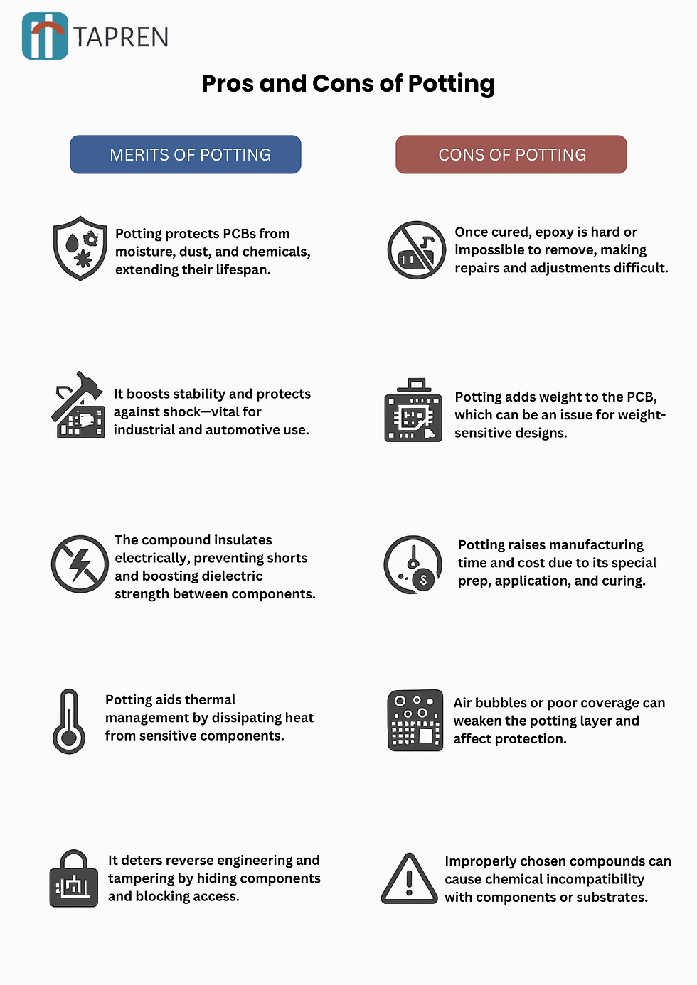
Merits of Potting
Potting is effective in protecting against moisture, dust, chemicals, and other environmental threats, extending the life of the PCB.
It provides mechanical stability and shields the components from shock and vibration, which is necessary in industrial or automotive applications.
The compound acts as an electrical insulator, preventing short circuits and enhancing the dielectric strength between components.
Potting can aid thermal management by helping to dissipate heat away from sensitive parts.
It prevents reverse engineering and tampering by concealing the components and rendering the board inaccessible.
Cons of Potting
Upon curing, materials like epoxy become difficult or impossible to remove, greatly complicating repairs and adjustments.
The material inserted adds to the weight of the PCB assembly, a consideration that can be troublesome to weight-conscious designs.
Potting increases manufacturing time and cost due to unique preparation, application, and curing needs.
Air bubbles or poor coverage upon potting can compromise the integrity and function of the protective coating.
Some compounds may result in chemical incompatibility with specific components or substrates if they are not properly selected.
PCB Potting vs Conformal Coating
Aspect | Potting | Conformal Coating |
Protection Level | Provides a higher level of protection by fully encapsulating the PCB and components, making it ideal for extreme environments. | Offers lighter protection by coating only the surface of the PCB, which is effective for mild conditions. |
Environmental Resistance | Excellent resistance to moisture, dust, chemicals, vibration, and physical shock. | Provides good resistance to moisture and mild chemicals but is less effective against physical shock or extreme temperatures. |
Mechanical Stability | Enhances mechanical stability by immobilizing components, preventing movement and vibration damage. | Offers minimal mechanical stability; it does not immobilize components as potting does. |
Reworkability | Difficult to remove or modify once applied, making repairs or component replacement challenging. | Easier to remove and repair since the coating can be stripped away without damaging the PCB. |
Weight and Volume | Adds significant weight and volume due to the thick layer of protective material. | Adds minimal weight and volume as the coating is very thin and lightweight. |
Cost and Time | More expensive and time-consuming due to the need for precise application and curing process | Less costly and faster to apply compared to potting |
Thermal Management | Provides some heat dissipation but may not be as effective as conformal coatings in managing heat. | Better suited for heat dissipation as the thin coating allows for more efficient heat transfer. |
Case Studies
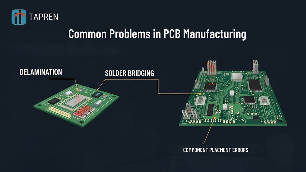
An experiment was conducted to investigate the encapsulation failure in the potting of an SMD transformer plastic housing. In the research, cracking, one of the most significant defects responsible for product rejection, was the area of interest.
Optical and electron microscopy were employed to study the soldered device, where cracks were noticed at the edges of the SMD transformer. Cross-sectional analysis also exhibited empty spaces around the cracks, i.e., that they may have been at the center of structural weakness.
Cracking was observed to propagate from the potting material to the plastic housing, particularly in the corner sections, indicating a need for improved potting quality and material strength.
Applications and Industry Use Cases

Potting is often used to protect electronic components against environments where moisture, vibration, and contamination are issues. Its strong protection has become widespread in various industries.
Potting is used in the automotive industry to protect sensors and control units against heat, vibration, and road shock.
Potting is utilized by the military and aerospace industry for the protection of electronics against severe temperature changes and pressure changes.
Industrial controls, such as motor drives and controllers, are often potted to ensure reliability in harsh environments with high dust and vibration levels.
Equipment used in renewable energy, such as solar inverters, employs potting for UV and moisture resistance.
Medical devices are shielded from potting to avoid internal electronics from damage due to bodily fluids and motion.
Marine electronics rely on potting for waterproofing and protection against corrosion.
Potting is applied to rugged products, such as waterproof smartphones and activity trackers, for consumer devices.
Industry Standards

Potting materials and procedures must comply with industry standards of safety, reliability, and adherence to regulations. The standards give manufacturers the guidance to select appropriate materials and apply them correctly.
IPC-CC-830 details the qualification and performance of conformal coatings and is typically applied in conjunction with potting practice.
UL 94 rates the flammability of plastic materials, and this is a key consideration in selecting potting compounds for safety-critical applications.
MIL-STD-454 provides general environmental requirements for military electronic equipment, including potting requirements.
Compliance with RoHS (Restriction of Hazardous Substances) dictates that potting compounds do not contain any hazardous materials, such as lead or mercury.
REACH (Registration, Evaluation, Authorisation and Restriction of Chemicals) mandates the documentation and safe handling of chemical substances contained in potting compounds sold in the European Union.
Key Takeaways
Potting is a well-established and widely used method of protecting printed circuit boards (PCBs) against environmental stress, mechanical failure, and electrical failure. Through total encapsulation of the circuit, it achieves long-term reliability in applications ranging from automotive to aerospace.
While potting offers significant benefits in terms of protection and stability, it also presents challenges in terms of cost and reworkability. With constant developments and conforming to industry standards, potting technologies are evolving to match the current electronic demands. Its applications, processes, and types must be well-understood for improved decision-making in electronic production and design.
Whether you're designing electronics for cars, factories, or outdoor environments, potting can make or break your product’s durability. At TapRen, we help you select the ideal potting compound and apply it correctly to safeguard your circuit boards against water, vibration, dust, and heat.


Comments