PCB Test Required in Manufacturing
- TapRen Team

- Mar 11
- 5 min read
Updated: Apr 15

Introduction
Would you like your electronic devices to work perfectly every time? In that case, always start by making sure that the PCB inside the device has been thoroughly tested. PC board testing is a critical step in the manufacturing process that identifies issues such as shorted connections, component mismatches, and faulty solder joints. Poor board testing could result in complete failures. PCBs must be tested by their manufacturers to ensure they are stable, safe, and usable in real-world applications. Being aware of the basic concept, one will understand why PCB testing must be carried out, how it is conducted, and the problems producers encounter.
Why is PCB Testing Necessary in Manufacturing?

PCB testing is highly considered a key procedure that ensures the quality, reliability, and safety of electronic products. It ensures that each board meets specific design requirements, is stable, and that the system is free from component defects. Costly setbacks, recalls, and safety hazards, especially in safety-critical applications such as motor vehicles and medical devices, can be easily mitigated by PCB testing. Furthermore, it also enables industry standards by minimizing manufacturing expenses through early fault detection, fewer corrections, and delivering quality products to the users.
Key Objectives of PCB Testing

PCB testing is a critical manufacturing component that checks for defects, ensures quality, and confirms the board works as expected before installation. Some principal objectives of PCB testing are mentioned below;
Checking electrical conductivity and short circuits, as well as open circuits, for signal flow.
A thorough inspection of mechanical and environmental resilience enables the board to withstand stress, temperature, and humidity.
Validate the correct alignment and orientation of components to prevent functional defects.
Securing solder joint quality and cleanliness, with no defects or contamination.
Testing of the general board operation to verify reliable performance in normal use conditions.
Common Types of Testing
PCB testing is necessary to confirm that the circuit boards work properly and are free from defects. Below are five of the most common and used PCB testing methods;

In-circuit testing utilizes a specialized fixture with probes that contact various points on the PCB. Each component is tested separately, regardless of the power status. It is precise, fast, and well-suited for high-volume manufacturing, used for detecting faults such as misplaced components and weak connections.
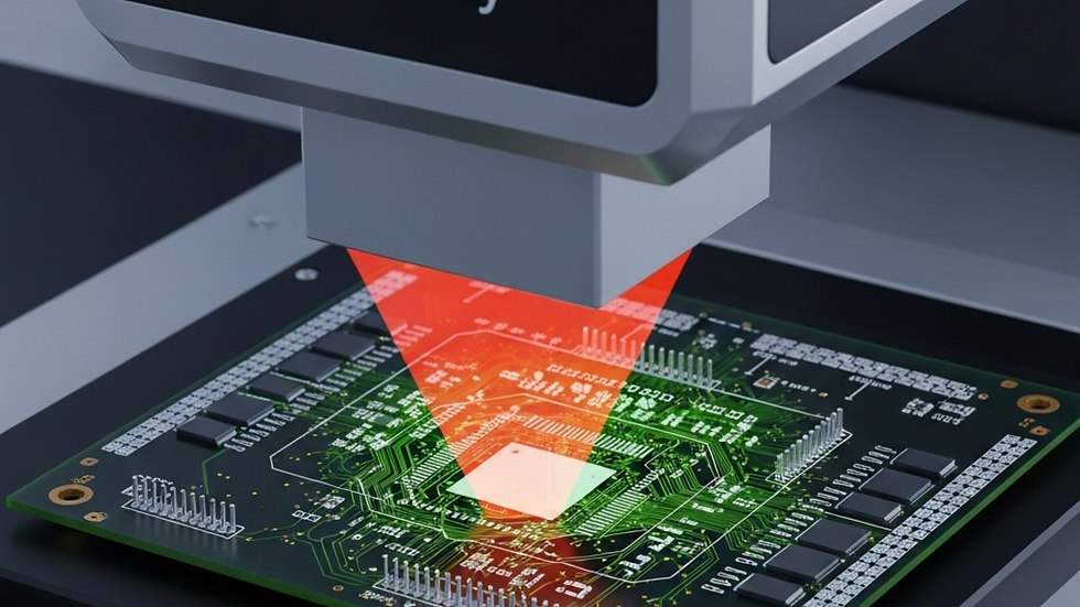
Automated Optical Inspection (AOI)

AOI uses cameras to examine the PCB's surface. They test for lost and displaced parts, soldering mistakes, and small visual defects. There is no risk of damaging the board as AOI is fast and contactless. It is mostly used after soldering.
Flying Probe Testing
Flying probe testing uses movable probes that touch different points on the board. It ensures periodic checks for shorts, open circuits, and component values. Flying probe testing takes a longer period of time, whereas ICT is considered more versatile and cost-effective for small to medium production or prototypes.

X-Ray Inspection
X-ray inspection is necessary when you want to see inside the PCB or inspect elements hidden under components, such as Ball Grid Arrays (BGAs). It identifies problems like hidden soldering defects, internal cracks, and solder gaps. It is typically used to inspect high-density or complex printed circuit boards.
Functional Testing
Functional testing confirms PCB functionality before shipping. The board is powered and tested in real-world conditions in the same form as the end product. It identifies issues that other tests do not, specifically the functionality of the entire circuit.

Visual Inspection
Visual inspection is one of the simplest forms of PCB inspection. It is either manual, conducted by experts, or aided by magnification tools. It looks for faults that can be detected by the naked eye, including misaligned components, cracked traces, or faulty solder joints. It is effective for critical points and early verification.

PCB Testing Standards

PCB testing is conducted in accordance with industry standards and certifications that ensure quality, safety, and reliability. Listed below are a few common certifications necessary for PCB testing;
Standard Certification | Purpose |
IPC-A-610 | Sets precise criteria for acceptable soldering quality and electronic assemblies. |
J-STD-001 | Sets out specific requirements for solder material, soldering process, and manufacturing quality. |
MIL-STD-883 | Requires thorough test procedures for microelectronic devices to meet military specifications. |
ISO_9001 | Provides a quality management guide to help maintain constant production and testing. |
UL Certification | Ensure products comply with safety and fire-protection standards for electronics. |
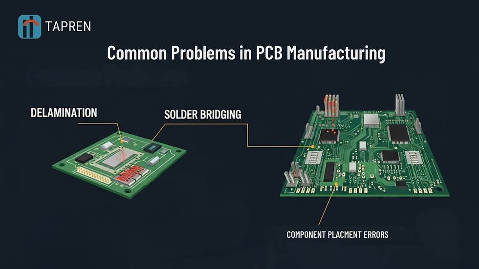
Frequent Testing Issues in PCB Manufacturing

PCB testing may encounter multiple problems due to complex designs, microcomponents, and high-quality requirements. Familiarity with potential problems enhances test accuracy and the reliability of the end product.
Miniaturization and High Component Density
As devices become smaller and more powerful, components are packed tightly. This makes it harder to access test points and increases the risk of undetected defects.
Complexity of PCB Designs
Complex designs require advanced testing strategies and equipment. Modern PCBs often feature complex layer setups, high-speed signals, and integrated signal components.
Variability in Components
Component tolerance, pirated parts, or inconsistent supply quality can lead to performance variation. Testing helps alleviate these issues before the product is shipped.
Testing Cost and Time
Especially in small batches, extensive testing can relatively increase production time and cost. Moreover, there’s always a constant balance between test coverage and manufacturing efficiency.
Adaptability to New Technologies
The latest innovations and modern standards should be updated to reflect the evolving technologies of today. Flexible PCBs, High-Density Interconnects, and advanced packaging should be incorporated.
Environmental Challenges
Aligning PCB testing with environmental conditions, such as high humidity, extreme temperatures, and vibration, can be costly and time-consuming, but it is vital for durability assessments.
Conclusion
PCB testing is not a step but a critical process during production that ensures product performance, reliability, and safety. Over time, electronics have become increasingly complex and smaller, making thorough testing even more critical. Each method plays a critical role in the early detection of defects, minimizing costs, and upholding brand image, from visual inspection to automated equipment and stress testing. Investing in high-quality PCB testing ensures enhanced product performance and a more satisfying user experience.
FAQs
Is the PCB test automated?
PCB tests can be automated using machines such as AOI, ICT, and flying probe testers. There may be a need for special tests or manual verification, particularly in the latest designs or complex boards that require a human touch.
Which aspect of PCB is tested in a PCB?
Typically, a PCB is verified for correct electrical connections, absence of shorts or opens, correct component installation, good soldering, and proper functionality. Tests also verify defects such as cracked traces, missing components, or low-quality solder joints, ensuring the board functions as intended.
How frequently should test equipment be calibrated?
The PCB test machines require recalibration every 6-12 months. It will ensure the machines exhibit correct results and that test quality is repeatable, helping to reduce errors in faulty end-products.
How do you test miniaturized or dense PCBs?
It is verified through extremely advanced techniques, including boundary scans, flying probe tests, and X-ray tests. It provides access to invisible or inaccessible test points that cannot be reached through traditional methods.


Comments