PCB Warpage and its prevention
- TapRen Team

- 6 days ago
- 8 min read

Introduction
How can a PCB be designed so that it is perfectly flat, but when one attempts to assemble the PCB, it bends or twists or refuses to lie flat? This effect is PCB warpage, which can be defined as "the condition where a printed circuit board (PCB) has a non-flat form that occurred after being manufactured". Although it may seem trivial, it is a major challenge for manufacturers and assemblers. Poor solder joint quality, uneven component alignment, assembly slowdowns, or failures are some key effects of PCB warpage. PCB warpage is a manufacturing quality issue resulting from poor design; even tiny warpage can affect PCB yield and ultimately reliability. This article covers the definition, causes, and effects, detection methods, and ways to prevent PCB warpage during PCB manufacturing.

What is PCB Warpage?
PCB warpage is a type of geometric distortion caused when a printed circuit board does not remain in a flat position as expected. PCB warpage can take the form of upwards bending (convex), downwards bending (concave), or diagonal twisting. Thermal and mechanical stresses from both manufacturing and assembly processes cause warpage in bare printed circuit boards (PCBs) and in assembled printed circuit board assemblies (PCBAs). Lamination processes will cause some PCB warpage, but if it becomes excessive, the PCB is considered defective. IPC standards (IPC-6011 and IPC-6012) specify accepted levels of warpage for PCBs and PCBAs. Generally, they do not exceed 0.75% of the PCB's diagonal; their limits are much lower for highly accurate components.
Types of Warpage

PCB warpage can occur in different shapes depending on the board's bending or twisting. Recognizing these common types helps in understanding the cause of deformation and choosing the right corrective action.
Boing
Bowing occurs when a PCB bends along its length or width rather than remaining flat. In some cases, the center of the PCB will lift or fall, while the sides remain straight, but this is most common in very large/thin PCBs.
Twisting
Twisting occurs when the corners of a PCB lift at different heights, creating a diagonal shape rather than a flat one and causing misalignment during component placement and soldering.
Saddle
Saddle warpage occurs when the PCB curves in multiple directions simultaneously. Both diagonals of the PCB can lift and sink, causing uneven mechanical stress across the PCB surface.
Arching
Arching results from heating or cooling an unevenly manufactured PCB in which the corners are lower than the center, giving the board a convex shape, like a bowl.
Bowl
Bowl warpage is similar to arching, except that the lower edges rise, creating a bowl-like shape on the PCB that negatively affects solder joint quality and component reliability.
How does PCB Warpage Occur?

CB warpage results from thermal and mechanical stresses arising from factors such as manufacturing errors, environmental exposure, and material mismatches. A PCB board can become permanently deformed due to repeated heating and cooling and improper handling, which can gradually introduce internal stress into the board. There are several causes listed below;
PCB Fabrication-Related Factors
Processing conditions during manufacturing include high pressure and drying during PCB lamination. Additionally, stress and rapid cooling during reflow soldering after PCB drying, as well as residual stress within the PCB, can result in warping. As the PCB undergoes thermal cycling during manufacturing, warpage can develop due to thermal expansion.
Another major factor that can contribute to PCB warpage is the use of asymmetrical laminated or copper-layered boards, which can create thermal imbalances that manifest as twisting forces in the PCB.
Post-Manufacturing Effect and Environmental Factors
Whenever a PCB is exposed to moisture, it may warp due to Virtual Drying. PCBs may also warp due to stress from high-temperature cycling after assembly (especially those that are not lead-free).
Material-Related Causes
This is one of the major causes of PCB warpage. Copper and FR-4 expand at different rates when heated due to different coefficients of thermal expansion (CTE). During high-temperature processes, material differences cause internal stress.
Quantifying PCB Warpage
Warpage is usually measured as a percentage of the board's size.
A common formula used is:
Warpage (%) = (Maximum deviation from flat / Board length) × 100
Industry standards (like IPC) typically allow:
≤ 0.75% warpage for surface-mount assemblies
≤ 1.5% warpage for simpler assemblies
Boards exceeding these limits may fail assembly or reliability tests.
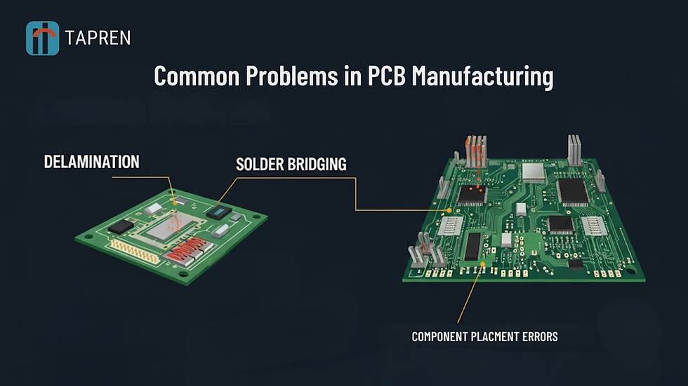
Effects of PCB Warpage

The way a PCB warps during the manufacturing process will affect its manufacturability, electrical characteristics, and long-term reliability.
Warpage-Impacting Solder Joint Quality
During reflow soldering, warpage generally increases at peak temperatures, causing components to lift, shift, or detach from the PCB. This results in defects such as, but not limited to, tombstoning, head-in-a-pillow, and cold-solder joints. Similarly, when soldering with wave soldering, if the board has warpage, it may not align properly with the solder wave, resulting in incomplete soldering.
Warpage impacts the accuracy of your assembly
PCB warpage can affect the accuracy of automated SMD assembly, as the pick-and-place machine cannot place parts correctly on a non-flat surface. During solder paste printing, warped PCBs reduce contact between the stencil and the PCB, potentially resulting in uneven solder paste deposits.
Warpage-Impacting Electrical & Mechanical Reliability
Residual stress in printed circuit boards can also cause solder joint fatigue during PCB thermal cycling. This phenomenon may cause microcracks to form, leading to intermittent electrical failures. Warpage may also cause uneven mounting stress, damage components, and improper PCB mounting.
Impact on Cost and Yield
PCB warpage can increase manpower, time, and cost for rechecking the boards. In most cases, Slowdowns after assembly, declining reliability, and field returns can increase production costs and reduce overall manufacturing yield.
Design Considerations

Proper PCB Design is the best way to prevent PCB warpage. A PCB designer should carefully consider the balanced distribution of copper across the PCB layers to maintain proper thermal expansion. If Copper distributions cannot be equalized, the PCB designer should incorporate non-functional fill to compensate for uneven copper distribution.
PCB Layer Symmetry will help reduce PCB bending more effectively during thermal cycling. The PCB designer must match the copper weight across the corresponding PCB inner-layer stack-up. The correct thickness will be determined by how much taller the PCB is; the taller the PCB, the thicker it needs to be to minimize warping.
Additionally, choosing the right PCB materials with a high glass transition temperature (Tg ≥ 170°C) ensures they remain rigid throughout various manufacturing steps. Materials like. Uniform copper foil thickness and controlled resin content help maintain stable thermal expansion and mechanical behavior across the board.
Mitigation Techniques for Existing Warpage

When PCB warpage occurs, controlled corrective measures are needed to restore flatness without affecting reliability. Depending on the severity of warpage, thermal, mechanical, or rejection-based approaches are used.
Thermal Flattening Cycles
Thermal flattening is commonly used to correct mild PCB warpage. The board is heated to a controlled temperature near its glass transition temperature (Tg) and then slowly cooled while held flat. This process allows internal stresses to relax and for deformation to redistribute. Thermal flattening is most effective for bare boards or lightly assembled PCBs. However, excessive heat exposure may degrade materials or solder joints, so process control is critical.
Mechanical Presses with Vacuum
Mechanical pressing combined with vacuum is used when thermal methods alone are insufficient. In this technique, the warped PCB is placed between flat plates under controlled pressure while a vacuum removes trapped air. The applied force gradually restores flatness without introducing additional stress. This method is effective for moderate warpage but is less suitable for densely populated boards, as excessive pressure may damage components or solder joints.
When to Reject vs. Rework Panels
Not all warped PCBs should be corrected. Boards within acceptable warpage limits and without solder joint damage may be reworked safely. However, panels that exceed IPC warpage limits or show cracked solder joints, lifted pads, or component stress should be rejected. Reworking severely warped boards can introduce hidden reliability risks, making rejection the safer and more cost-effective option.
Prevention Methods for PCB Warpage

Preventing PCB warpage requires careful control of design, materials, thermal exposure, and handling practices. Addressing these factors early in the manufacturing process helps maintain board flatness and improves overall reliability.
Controlled Thermal Processing
Managing temperature changes during manufacturing is essential to prevent warpage. Reflow soldering profiles should be optimized to ensure uniform heating and cooling. Reducing thermal gradients minimizes uneven expansion, while proper thermal relief structures help distribute heat more evenly across the PCB board.
Balanced Board Architecture
A well-balanced PCB layout reduces mechanical stress. Components should be evenly placed, and copper layers should be designed symmetrically. Using mirrored layer stack-ups and consistent copper thickness across layers ensures uniform expansion and contraction during thermal cycling.
Selection of Stable Materials
Using materials with compatible thermal properties greatly reduces the risk of warpage. High-quality FR-4 substrates provide good dimensional stability for most applications, while high-Tg laminates are suitable for high-temperature processes. Proper thickness selection is also important, as very thin boards deform more easily.
Copper Density Management
Maintaining similar copper coverage on complementary layers helps prevent bending. Copper pours can be added to low-density areas to balance the layout. When adding copper fills, design rules must be followed carefully to avoid electrical interference or impedance mismatches.
Moisture Control Before Assembly
Moisture absorbed by PCBs can expand rapidly during heating, increasing warpage. Pre-baking boards before assembly removes trapped moisture and relieves residual stress in the laminate, reducing deformation during soldering.
Proper Storage and Handling Practices
PCBs should be stored flat in clean, dry, and temperature-controlled environments. Panels must be properly supported and handled carefully to avoid bending. Poor storage or rough handling can introduce warpage even before the assembly process begins.
Conclusion
PCB warpage is a critical challenge that affects every stage of printed circuit board manufacturing, from design and assembly to long-term product reliability. Understanding its causes, types, and measurement methods helps engineers make informed decisions during material selection and board design. By applying proper design practices, controlling manufacturing processes, and using effective prevention and mitigation techniques, warpage can be minimized. Early detection and proper handling of warped boards not only improve assembly yield but also ensure the reliability and durability of electronic products.
FAQs
1. How to check PCB warpage?
PCB warpage can be checked by measuring the maximum deviation of the board from a flat reference surface. Tools such as flatness gauges, dial indicators, laser scanning systems, and moiré fringe methods can be used to measure PCB warpage. The measured deviation is then compared to the board’s diagonal length to calculate the warpage percentage.
2. What are the PCB warpage standards?
PCB warpage standards are defined primarily by IPC specifications, including IPC-6011 and IPC-6012. For surface-mount assemblies, the typical allowable warpage limit is 0.75% of the board diagonal, while through-hole boards may allow up to 1.5%. High-reliability applications often require stricter limits.
3. Does PCB thickness affect warpage?
Yes, PCB thickness significantly affects warpage behavior. Thinner boards are more flexible and more likely to warp during thermal processing. Thicker boards provide greater stiffness and resistance to bending, especially for large boards. However, very thick boards can trap internal stress if not properly designed and manufactured.
4. How can I detect PCB warpage early in production?
Early detection of PCB warpage can be achieved by inspecting boards after lamination and drilling, and before assembly. Flatness gauges, laser measurement tools, and automated optical inspection systems help identify deformation early. Detecting warpage at early stages prevents costly rework or scrap during final assembly.
Next Read:
Carbon Fiber PCB


Comments