
Why Introduce Graphene into Advanced PCBs?

Updated: Jul 22

Are you experiencing problems with your existing printed circuit board (PCB) designs because they do not perform adequately (i.e., too slow, produce too much heat), and/or you want to design a lightweight/strong PCB?
Most industries have problems using traditional FR-4 PCB material because it has poor thermal interface, unreliable high-frequency signal transmission, and cannot meet the required mechanical properties to support structural integrity during long-term operation under extreme environmental conditions. Traditional PCB production methods do not provide the level of reliability and dependability needed to develop future generations of electronic devices and emerging technologies such as high-bandwidth communication systems, Aerospace, and High-Density Computing.
There is a growing body of research and engineering interest in alternative PCB technology based on non-traditional PCB material types, which may be limited by their cost, performance, and reliability. The combination of its superior electrical conductivity, thermal conductivity, and mechanical properties makes Graphene a viable candidate for developing PCBs with higher reliability than traditional PCBs to better withstand stresses and strains imposed upon them due to the heat generated by an operating device, the signal transmitted through the device, and the mechanical forces applied to the device. Graphene can be used in the development of PCBs as a conductive trace, substrate layer, and thermal interface material (TIM). Using Graphene to develop PCBs allows for reduced PCB weight, controlled PCB temperature, and improved PCB signal quality in applications where these characteristics are important. As a result, many researchers and manufacturers are exploring Graphene as a possible solution to improve performance and reliability in electronic systems.
Understanding Graphene in PCB Engineering
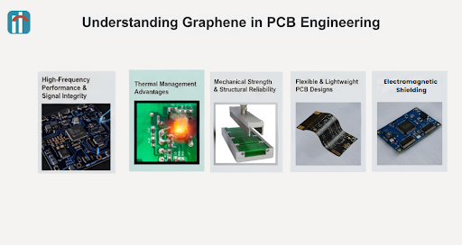
Graphene consists of a single layer of carbon atoms arranged in a hexagonal lattice. Although graphene has an extremely small thickness (micron level), it has some very interesting physical characteristics:
Higher electrical conductivity than most conventional materials
A thermal conductivity much better than copper
High tensile strength and high flexibility
Very light and strong structures
In PCB design, graphene can be found as:
Hybrid conductive coating layers
Thermal management films
Additives for substrate reinforcement
Materials for electromagnetic interference (EMI) shielding
Graphene is generally added to PCBs to complement copper traces and enhance their performance rather than replace them entirely.
High-Frequency Performance and Signal Integrity
As frequency increases into GHz and mmWave bands, copper interconnects are subject to increasing loss (skin effects and surface roughness). The high carrier mobility of graphene enables higher signal propagation efficiency at high frequencies.
In RF and high-speed digital circuit board design, the introduction of graphene will allow:
Decrease of Insertion Loss in Transmission Lines
Increase Impedance Uniformity among Traces
Decrease Electromagnetic Interference Between Layers
The characteristics of graphene make it highly appealing for high-end applications such as Phased-Array Antennas, Radar Modules, and Next-Generation Wireless Systems.
As an engineer, I know that a smooth, conductive graphene surface maintains signal integrity as signals travel through multilayer boards with a high trace density.
Thermal Management Advantages
One of the biggest challenges to building modern printed circuit boards (PCBs), is managing thermal issues. Today’s electronics generate large amounts of heat in small areas from powerful processor cores, power amplifier outputs, and densely packed sensor arrays, which traditional substrate materials cannot efficiently dissipate or manage.
Graphene is one of the most thermally conductive materials ever tested, with thermal conductivity many orders of magnitude higher than copper, and is an excellent material for heat spreading. Therefore, when integrated into either a ground plane or a thermal interface layer, it will enable uniform heat dissipation across the entire board.
The major advantages of using graphene in a PCB include:
A reduction of thermal hot-spots
Increased component reliability due to longer life.
Increased ability to handle increased power
Engineers creating compact electronics or developing high-power RF systems now have a way to improve the thermal efficiency of their designs without adding significant thickness to their boards.
Mechanical Strength and Structural Reliability
Most advanced PCBs are subjected to extreme environmental conditions that cause gradual degradation of their mechanical integrity and reliability due to cyclic thermal expansion and contraction, vibrations, and mechanical stress. The closely packed carbon atoms within a graphene material's lattice provide significant mechanical reinforcement to PCBs, thereby increasing their resistance to cracking and delamination over time. Graphene enhances both the flexural strength of composite laminates and the protective coatings used on these laminates, improving the laminates' resistance to oxidation and corrosion; however, the most significant impact of graphene is its ability to enhance long-term structural integrity and maintain consistent performance and reliability. Therefore, graphene-enhanced PCBs will be best suited for those applications that require consistent performance and longevity, such as aerospace electronics, automotive sensing systems, and industrial monitoring systems.
Enabling Flexible and Lightweight PCB Designs
Flexible electronics have a wide range of applications in wearable technology, biomedical sensing, and miniaturized communication systems. Metal traces in traditional printed circuit boards (PCBs) can fail under repeated flexing or bending.
The ability to fold and stretch makes graphene an ideal candidate to provide ultra-thin, ultra-lightweight PCB designs with excellent electrical properties. Designers and engineers will have the opportunity to develop:
Circuits that can be folded
A sensor interface that can be stretched
Modules for lightweight antennas
Due to its mechanical robustness, which allows it to maintain performance even under physical strain, graphene opens up entirely new opportunities for designers and engineers to develop flexible electronic architectures.
Electromagnetic Shielding and Noise Reduction
Graphene's unique characteristics make it suitable for use as a shield in high-density PCB layouts, particularly in designs involving high-frequency and/or mixed-signal components. The high electrical conductivity and layered thickness of graphene enable it to efficiently absorb and redistribute unwanted electromagnetic energy. In addition, when used as a coating, embedded layer, or part of the ground plane of a PCB, graphene has been shown to reduce crosstalk between adjacent traces, improve efficiency by reducing surface resistance, and enhance overall electromagnetic compatibility. All of these features help to provide for cleaner signal transmission and improved stability in RF, high-speed digital, and mmWave electronic systems.
Manufacturing Challenges and Considerations
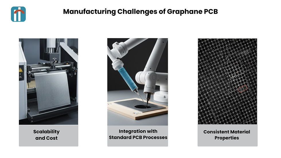
Graphene's potential for incorporation into various manufacturing processes related to printed circuit board (PCB) production is significant. However, for all but a few engineers and manufacturers attempting to create graphene-based PCBs, numerous technological and manufacturing issues will arise.
Scalability and Cost
Currently, creating large quantities of quality graphene is extremely challenging and costly. Because the deposition of graphene onto an appropriate substrate (CVD) or the separation of graphene from a graphite material both require precision, and because the cost of such precision is significantly greater than the cost of copper used to manufacture PCBs, many designs currently under development involve a hybrid approach where copper and graphene are combined. This allows designers to leverage graphene's unique properties while keeping manufacturing costs reasonable.
Integration with Standard PCB Manufacturing Processes
Manufacturing methods utilized to produce graphene-based PCBs differ from those utilized to produce traditional copper-based PCBs. Methods, including temperature management, surface preparation, and adhesive bonding, will likely need to be modified to ensure that the thin graphene layers are protected from damage or dislodgment during manufacturing. Research continues into the development of graphene-based printable inks and nanocomposite substrates to facilitate the easier integration of graphene into existing manufacturing workflows.
Consistent Material Properties
A major issue with integrating graphene into large-scale PCB manufacturing is maintaining consistent material thickness and electrical properties over long lengths. Material defects due to variations in material quality, grain structure, or layer distribution can affect the conductivity and high-frequency performance of the final PCB product. Therefore, maintaining tight process control and implementing advanced inspection techniques will be critical to achieving consistently reliable results when manufacturing graphene-enhanced PCBs.
Graphene’s Role in Next-Generation Electronics
The continued advancement of manufacturing processes will enable wider adoption of graphene in modern electronic systems. Due to its unique physical characteristics, including electrical, thermal, and mechanical properties, graphene will be suitable for use in a number of emerging technologies, including ultra-high-frequency communications equipment, high-density artificial intelligence computing platforms, flexible biomedical devices, and high-performance radar and sensing systems. The addition of graphene to printed circuit boards (PCBs) is not merely an upgrade to the material; it also opens new opportunities for nanoscale PCB design, enabling the redesign of future electronic systems with optimized, miniaturized performance and overall efficiency.
Conclusion
Graphene has been added to advanced PCBs to address major obstacles in today's electronics, including thermal issues with high-frequency signals, mechanical durability, and other thermal challenges. Research is ongoing, and while it will take time for this technology to be fully adopted, graphene-enhanced circuit boards could change how we think about future printed circuit boards.
Engineers designing new electronic products that are lighter, faster, and better at dissipating heat may find graphene an exciting option as they look to the future of printed circuit boards.
FAQs
1. Can graphene entirely supplant all copper in printed circuit board (PCB) designs?
No, most PCB designs that utilize graphene will continue to use both copper and graphene to enhance the PCB's thermal and high-frequency properties, rather than simply substituting one for the other.
2. In what ways does graphene improve high-frequency PCB performance?
Graphene's high electrical conductivity and very smooth surface help minimize signal loss, crosstalk, and electromagnetic interference in radio-frequency and high-speed circuits.
3. Are graphene PCB products available commercially?
Graphene PCB products are becoming commercially viable for specific applications; however, widespread commercial viability will be achieved as manufacturing advances.


Comments