How much Copper to use in PCB
- TapRen Team

- Nov 3, 2025
- 5 min read

Abstract
When a high-flying drone malfunctions in mid-air, the issue is generally not a component failure, but rather a result of insufficient copper thickness. In electronic devices like smartphones and medical devices, selecting the correct PCB copper thickness is crucial for normal operation and preventing disasters. Copper traces transfer all electrical power and signals on the circuit board, with thickness affecting current capability, heat, and signal integrity. This article provides an in-depth look at PCB copper thickness measurement and offers tips on selecting the appropriate specifications for various applications. These measures also help prevent costly mistakes that lead to redesigns or field failures.
Understanding Copper Weight and Thickness in PCBs
Generally, PCB copper thickness is misinterpreted as weight, as it is expressed in ounces per square foot (oz/ft²). This is often misinterpreted as PCB thickness and should not be confused during the original manufacturing process. The standard (1 oz) copper is a little over 1.4 mils (0.035 mm) thick, which is roughly the size of a hair.
A conversion table for reference is given below;
Copper Weight | Thickness (mils) | Thickness (mm) | Thickness (μm) |
0.5 oz | 0.7 mils | 0.017 mm | 17 μm |
1 oz | 1.4 mils | 0.035 mm | 35 μm |
2 oz | 2.8 mils | 0.070 mm | 70 μm |
3 oz | 4.2 mils | 0.105 mm | 105 μm |
Why does PCB Copper Thickness Matter?

PCB copper thickness is important because it determines how effectively the board conducts electricity, dissipates heat, and withstands other stresses. Thicker copper allows more current to flow, thereby reducing the risk of overheating and increasing the board's resilience. It also prevents the device from failing, especially when using high heat or high power. The thickness of the PCB makes it more rigid and resistant to bending.
Choosing the Right PCB Copper Thickness

In the selection of PCB copper thickness, the following factors should be considered.
Current Carrying Capacity
More current demands a thicker copper layer in the PCB. Use IPC-2221 guidelines or web-based calculators to calculate the minimum width of your trace and the required copper thickness for the current.
Thermal Requirements
Applications that require high heat or power require more copper to maintain the correct PCB thickness, which facilitates heat dissipation.
Mechanical Strength
Devices that are constantly in use should be strong enough to endure high shock and vibration. Such tools require more PCB copper thickness.
Design Density
Higher traces and spacing mean the density of copper should be used in PCB thickness. This can limit the high-density design.
Cost and Manufacturing Complexity
Higher copper increases material costs and makes etching and plating more challenging. Hence, complexity performance interferes with the costs and complexity of the design.
PCB Copper Thickness vs Current
The amount of current a PCB trace can safely carry depends on its width and the thickness of the copper.
Copper Weight(oz) | Thickness (mils) | Thickness (mm) | Recommended Current Range(A) | Best Applications |
0.5 | 0.7 | 0.017 | < 1 | Low-power signals, space-constrained designs, and mobile devices |
1 | 1.4 | 0.035 | 1-3 | Standard applications, signal layers, and most consumer electronics |
2 | 2.8 | 0.070 | 3-7 | Power distribution, industrial controls, and LED lighting circuits |
3 | 4.2 | 0.105 | 7-10 | High-current applications, power supplies, and automotive systems |
4 | 5.6 | 0.140 | 10-15 | Heavy power distribution, motor controllers |
Copper Weight Distribution for High-Performance Applications
Material selection and copper weight distribution are crucial steps for achieving high-performance applications.
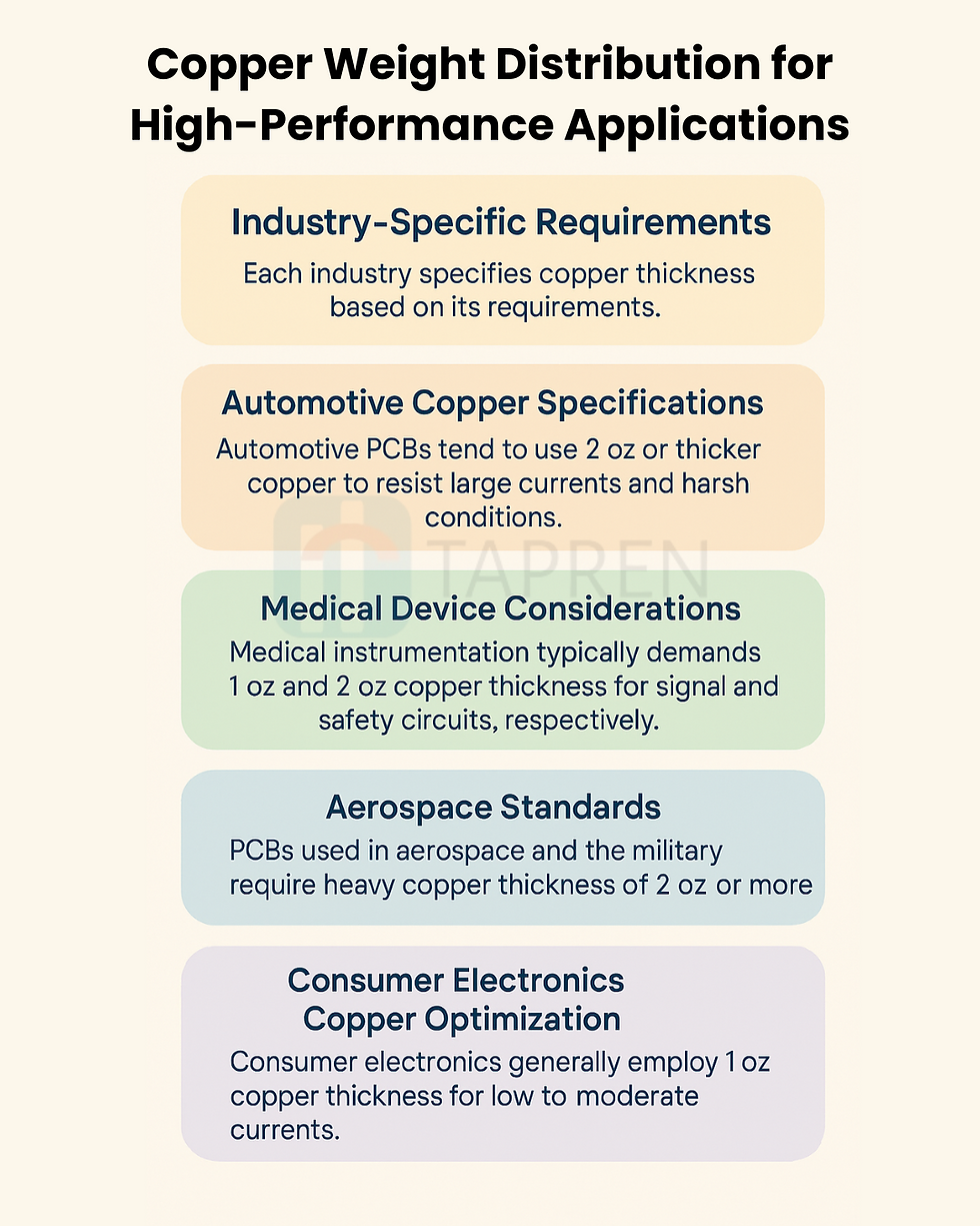
Industry-Specific Requirements
Each industry specifies copper thickness based on its requirements. For example, the automotive and aerospace industries require strength and carrying capacity, while medical devices require reliability and accuracy. Comparably, consumer electronics prefer diverse cost reduction and miniaturization.
Automotive Copper Specifications
Automotive PCBs typically use (2 oz) or thicker copper to resist the effects of large currents and harsh environmental conditions, such as vibration and high temperatures. Increasing the PCB thickness enhances its reliability and safety for critical applications such as engine controls and electric power steering.
Medical Device Considerations
Medical instrumentation demands high accuracy, precision, and reliability. Therefore, copper thickness is chosen carefully, typically around (1 oz) for signal circuits and (2 oz) for power or safety circuits. Choosing the right PCB copper thickness requires careful consideration, as both space efficiency and electrical performance must be optimized alongside other manufacturing tolerances.
Aerospace Standards
PCBs used in aerospace and the military require a heavy copper thickness of around (2 oz) or more to support high power loads and withstand harsher environments. NASA-STD-8739.4 and MIL-PRF-31032 are two specifications that provide standards for the quality and thickness of copper, ensuring durability and maximum system integrity.
Consumer Electronics Copper Optimization
Generally, consumer electronics employ (1 oz) copper thickness as these products are less expensive than medical and industrial products. These PCBs are designed to handle low to moderate currents. The default thickness perfectly satisfies the requirements in small devices like laptops and phones, where efficiency and size are major issues.
Manufacturing Implications
PCB copper thickness affects how a PCB is built, meaning that increasing the copper thickness prolongs the etching time and widens the traces. This hinders the fabrication of complex PCB designs. Furthermore, it also impacts the hole plating, which ensures a solid connection between different layers of the PCB, and can cause the board to warp if copper is not balanced. Lastly, more copper requires more material, which increases the manufacturing cost; therefore, designers must balance performance needs against cost and manufacturing limitations.
Key Takeaways
This article provides a detailed description of selecting the appropriate PCB copper thickness during the PCB design process. The selection of PCB copper thickness has a direct impact on its performance, reliability, and safety. As emphasized above, the correct weight of copper helps control current, heat, and prolongs the long-term life. Various copper thicknesses are used in different devices, which affects the PCB design selection during manufacturing. In short, selecting the proper copper thickness is a prudent move toward creating stronger, safer, and more efficient electronic products.
FAQs
How much copper does my PCB require?
The amount of copper in a PCB depends on current-carrying requirements and design specifications. Standard PCBs will use (1 oz/ft²) of copper, which is heavily used about 35 microns of thickness. In systems with higher power demands, 2 oz or greater may be used to enable greater currents to flow and dissipate heat more effectively.
What should one assume when changing copper thickness if my PCB is overheating?
If a PCB heats up excessively, it is possible to enhance heat dissipation and current-handling capability by increasing the thickness of the copper. Switching to a higher layer of copper, such as 2 oz/ft² or 3 oz/ft², reduces the potential for thermal damage. Larger copper traces or adding thermal resistance through enhanced heat management that prevents overheating.
Is it appropriate to use various copper thicknesses on the identical PCB?
It is acceptable to use various copper thicknesses in identical PCBs, based on the requirements. This is widely followed in multi-layer PCBs, where thicker copper zones are planned for higher current-carrying sections or better thermal dissipation, and thinner copper is used for other sections with lower power consumption. Proper design practices ensure uniform performance.
How can manufacturing costs be reduced while getting good copper thickness for consumer products?
To reduce the cost of manufacture, use standard copper thicknesses, such as 1 oz/ft², and design a PCB model with a minimal copper area that does not compromise function. Effective design methods, such as reducing trace width or employing a smaller board size, can reduce costs while maintaining sufficient copper thickness to ensure reliable operation.
How does copper thickness affect my board's EMI/EMC performance?
The electromagnetic interference and electromagnetic compatibility of a PCB are defined by the copper thickness, which affects the board's heat transfer efficiency and dissipation property. Thick copper enhances shielding and reduces noise, whereas thin copper enhances resistance and results in weaker shielding. Optimizing copper thickness correctly helps to balance EMI/EMC problems for high-speed designs.


Comments