Innovations in PCB Manufacturing: Automation and Quality Assurance
- TapRen Team

- Jan 12, 2025
- 7 min read
Updated: Jan 21, 2025

Abstract
This article explores the latest innovations in Printed Circuit Board (PCB) manufacturing. While there are many innovations, we'll focus on the transformative impact of automation and quality assurance. You will learn about fancy techniques that make PCBs better and faster, common design mistakes to avoid (because even geniuses make mistakes sometimes), and the emerging role of AI in streamlining the design process. By the end, you'll have a solid understanding of how these innovations are shaking things up in the industry.
Introduction to PCB Manufacturing Innovations
Traditionally, PCB manufacturing involved meticulous manual processes (some companies still use that to date). Earlier, components were carefully soldered by hand, and inspections relied heavily on the human eye as documented in IPC-A-610 “Acceptability of Electronic Assemblies”. While these methods served their purpose, they were susceptible to human error and lacked the efficiency to meet the ever-increasing demand for high-performance electronics.
Why is Innovation Important?
The limitations of traditional methods became apparent with the miniaturization of electronic components and the demand for higher reliability. This resulted in a need for:
● Increased Precision: The miniaturization trend in electronics pushes the limits of manual assembly. Modern PCB manufacturing requires micron-level precision for solder ball placements on Ball Grid Arrays (BGAs) and High-density interconnect (HDI) PCBs. Placing them manually may lead to misalignment, shorts, and openings, and can hinder scalability for high-volume production.
● Reduced Human Error: Manual processes introduce inconsistencies like component misalignment, which can cause electrical shorts. Another inconsistency is weak solder joints due to improper application. Variations in heating are another inconsistency, and this impacts reliability.
● Enhanced Efficiency: The growing electronics industry demands faster production times to meet market needs. However, achieving fast time-to-market doesn't have to come at the expense of quality. Manual assembly processes may lead to production delays and unreliable products due to defects.
● Improved Quality Control: Human inspectors rely on their visual acuity and experience to identify defects. Individual differences in perception can lead to inconsistencies in defect detection. Also, manual inspection only sees the surface and not internal defects like hidden cracks. Manual methods hinder efficient defect data collection and trend analysis leading to non-compliance with standards, reduced reliability, and unhappy customers.
These factors paved the way for a wave of innovation in PCB manufacturing.

Recommended reading: The Evolution of PCBs in Modern Electronics: Enabling Innovation and Connectivity
Common PCB Design Mistakes
Even with the best manufacturing techniques, design flaws can still occur. Here are some frequent errors that can have a domino effect on PCB performance:

Incorrect Layer Stacking: PCB layers function as transmission lines with characteristic impedance, a property that defines the relationship between voltage and current. Incorrect stacking, like placing high-speed signal traces between ground planes with a large separation distance, creates an increase in the trace's effective capacitance. This disrupts the intended impedance of the trace (often controlled by trace width and dielectric spacing). Such impedance mismatch causes signal reflections at transitions and bends in the trace. These reflections travel back toward the source, corrupting the original signal and leading to data errors and potential malfunctions. For example, high-speed memory traces like DDR4 clocks need a sweet spot between power planes for power delivery. Too close creates excessive capacitance. Power plane voltage swings (switching) inject noise (crosstalk) into the memory signals, causing errors and data corruption.

Poor Thermal Management: During operation, PCBs generate heat like car engines, due to power dissipation in components like resistors, capacitors, and integrated circuits (ICs). Neglecting thermal management is like ignoring a car's cooling system. This uncontrolled heat elevates the junction temperature (Tj) of ICs, a metric for their health. High thermal resistance (θ) between the IC and the surrounding environment hinders heat transfer. If θ is high and Tj exceeds its limit due to insufficient cooling, premature aging, malfunctions, or even component failure can occur. For instance, an uncooled voltage regulator can overheat and shut down, rendering the entire circuit powerless.

Inadequate Spacing: Just like maintaining safe distances between electrical wires in your house, PCBs require a minimum clearance between conductive elements (traces, pads) to prevent short circuits. This spacing is crucial to avoid accidental contact between conductors. Imagine a smartphone's USB-C charging port. The tiny pins within the port connect to corresponding traces on the PCB. If these traces are too close together, a manufacturing defect or physical stress on the phone could create a bridge between them, causing a short circuit. This uncontrolled current surge, exceeding the intended rating of the traces or charging components, could damage the phone's charging circuit or even ignite the PCB material. In worst-case scenarios, this can lead to permanent phone damage or even a fire hazard.
Advanced Manufacturing Techniques
PCB manufacturing employs a range of processes and techniques designed to enhance miniaturization, performance, and reliability. To avoid the common mistakes in PCB manufacturing, you will have to employ advanced manufacturing techniques. This section spotlights two primary techniques: automation and quality assurance.
Automation is now at the forefront of PCB manufacturing, offering numerous benefits:
Increased Efficiency and Productivity: Automated machines can perform tasks significantly faster and more consistently than human workers, leading to higher production outputs.
Reduced Human Error: Robots eliminate the possibility of human error in tasks like component placement and soldering, leading to a higher yield of defect-free PCBs.
Cost Savings: While initial investments in automation can be high, the long-term benefits translate to reduced labor costs and improved production efficiency.
Examples of Automated Processes

Pick-and-Place Machines: These robots boast pinpoint accuracy and precision in component placement, ensuring each component is meticulously positioned on the PCB within a tolerance of typically 25 microns (µm) or less according to the IPC Class 3 design guide. This accuracy surpasses human capabilities and minimizes placement errors that could lead to assembly defects. Its eagle-eyed cameras, often exceeding 10 megapixels, capture intricate details of components on feeder trays. Also, its advanced systems leverage artificial intelligence, specifically deep learning algorithms, for intelligent component recognition and real-time error detection. This ensures only the correct components are selected. The encoders, acting as the eyes of the system, provide continuous feedback on the head's position, giving a real-time feedback loop that allows for immediate adjustments.

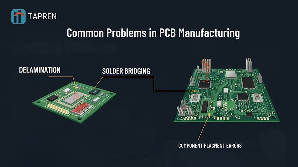
Automated Optical Inspection (AOI): Acting like digital detectives, these systems use high-resolution cameras and image recognition software to scrutinize every inch of the PCB. This inspection often identifies potential joint defects like excess solder, and insufficient or no solder which can lead to weak connections between Integrated Circuits (IC) and the PCB. This weakness can cause electrical resistance, leading to overheating, power fluctuations, and even complete component failure. Other defects that can be identified include lifted or bent leads which can cause intermittent connections, resulting in malfunction. Another defect is shifted components, causing misalignment with intended connection points, also leading to malfunction. Also, both bridged and pseudo solder joints appear well-formed but lack a proper metallurgical bond, leading to potential openings and malfunction under stress.

Robotic Soldering: Robotic soldering combines advanced vision systems and intricate control mechanisms to achieve consistent, high-quality connections. Its high-resolution cameras with sophisticated image processing algorithms help it meticulously identify and locate components on the PCB. Some systems even use artificial intelligence for real-time defect detection, ensuring only the correct components are targeted for soldering. Once identified, the robotic arm, guided by precise motion control systems, maneuvers the soldering iron with exceptional accuracy. Its linear motors provide smooth, high-speed movement with minimal vibration, ideal for forming delicate solder joints. The encoders constantly monitor the position of the soldering tip, allowing for real-time adjustments and guaranteeing consistent solder application within tight tolerances. This synergy between vision and control ensures reliable, repeatable soldering, surpassing human capabilities and minimizing the risk of errors like overheating, insufficient solder, or misaligned components. You can leverage IPC Standards to ensure soldering practices meet the stringent quality and reliability demands of the modern electronics industry. For instance, IPC-A-610 sets the bar for acceptable assemblies, IPC-J-STD-001 lays the groundwork for achieving that quality, and IPC-7711/7721 provides the tools for rectification when necessary.
Quality Assurance in PCB Manufacturing
While automation streamlines production, ensuring flawless PCBs requires a keen eye for detail. This is where advanced inspection techniques come in. These techniques are crucial for identifying defects early in the production process, preventing them from reaching later stages and causing costly rework or product failures.
Key Technologies in Quality Assurance

X-ray Inspection: This technology allows for a deeper look, revealing internal defects like micro-cracks in buried conductive paths, voids with the BGA solder joints, and component placement misalignment that may be covered by other components on the surface.

Automated Testing Equipment: These systems meticulously test every connection and function of the entire PCB assembly, guaranteeing it meets all the required design specifications for continuity, voltage levels, and signal integrity. This ensures the PCB functions without flaws under intended operating conditions.

In-Circuit Testing: This technique uses a bed of spring-loaded probes that make contact with designated test points on the PCB. It verifies the electrical continuity, functionality, and programmed values of individual components like resistors, capacitors, and integrated circuits. This ensures proper component assembly and functionality before further processing.
Benefits of Advanced Quality Assurance
Higher Reliability: PCBs produced with these methods undergo rigorous scrutiny, leading to a lower risk of failures and a longer lifespan.
Reduced Risk of Product Failures: Early detection of defects ensures that faulty PCBs are identified and addressed before they reach the final product stage.
Key Takeaway
Advanced manufacturing techniques, particularly automation and quality assurance, are essential in preventing common PCB design mistakes. They address the limitations of traditional methods, boosting efficiency, and precision, and eliminating human error. Automated processes like pick-and-place machines and AOI systems ensure consistent quality, while X-ray inspection and rigorous testing guarantee reliable PCBs. The future holds promise with flexible PCBs, 3D printing, nanotechnology applications, and continued progress in automation and AI.
TapRen, a leader in PCB innovation, leverages these techniques to enhance design precision, boost production efficiency, and ensure top-tier product quality. With TapRen's expertise, you can trust in creating innovative electronics that meet the highest industry standards. For more information on how we can support your PCB needs, visit TapRen.


Comments