Top 5 PCB Design Mistakes and How AI Can Help You Avoid Them
- TapRen Team

- Jan 21, 2025
- 10 min read
Updated: Jan 29, 2025

Abstract
This article dives into the top 5 PCB design mistakes that can plague even the most seasoned professionals. We'll explore issues like improper spacing and trace widths, and demonstrate how AI analysis tools can become your secret weapon for identifying and correcting these errors early in the design phase. By leveraging AI, you can prevent costly production delays and ensure your PCBs operate at peak performance.
Introduction
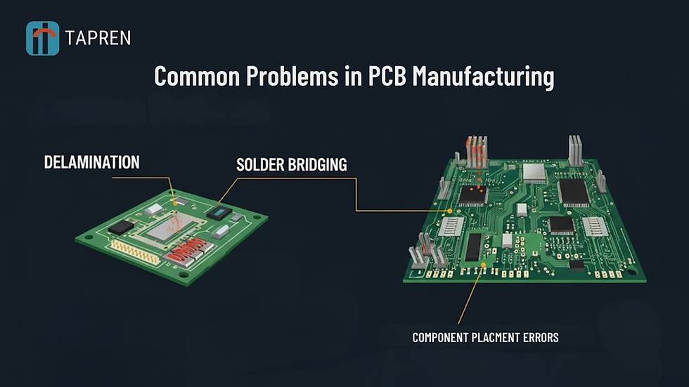
The technologies that create our modern world are made possible by the painstakingly built layers of a printed circuit board (PCB). Many of our modern devices, including smartphones and satellites, are built on the complex fabric of well-designed PCBs. These powerful designs are packed with electrical connections and carefully placed parts like resistors, capacitors, fuses, and transistors, all of which work together to ensure the device operates smoothly. The PCB as a whole will malfunction if one of these parts fails, which will impair the product's operation. Aside from that, frequent design errors can happen to even the most experienced design engineers. These mistakes can set off a series of problems that could lead to a disastrous product failure, manufacturing delays, or even a decline in performance.
Fortunately, the growing field of artificial intelligence (AI) provides a breakthrough for PCB designers. Engineers can now examine their ideas with unprecedented detail by using advanced AI techniques. These AI watchdogs can see problems early on and raise the alarm before they snowball into costly setbacks. Let's look into the top 5 PCB design mistakes and see how AI can help you avoid them.
PCB Mistakes and AI Solutions
1. Improper Spacing

Insufficient spacing between components and conductive traces can lead to two major problems;
Short Circuits: A short circuit occurs when an electrical current takes an unintended, shorter path instead of following the designated circuit. It is often due to too little space between conductive traces on a PCB. This accidental electrical connection makes it possible for current to flow through places it shouldn't, which could harm some parts of the device and lead to its failure. For instance, a short circuit on a smartphone's power delivery network could lead to a complete power outage, rendering the device inoperable.
Electromagnetic interference (EMI): Even with proper spacing, excessively close traces can create EMI. Imagine electrical exchanges occurring among components on a printed circuit board. When these exchanges cross over into one another, unwanted noise is introduced and signal integrity is compromised. RF circuits, which are crucial high-speed applications, are susceptible to electromagnetic interference (EMI), which can result in signal loss or data corruption. One potential cause of a shaky or weak internet connection is electromagnetic interference (EMI) on the PCB of a Wi-Fi module.
AI to the Rescue
AI-driven design tools can carefully examine your PCB layout and use complex algorithms to spot any possible spacing infractions. These instruments are capable of:
Compare trace spacing to industry standards: AI can guarantee that your design complies with minimum spacing standards based on voltage ratings, trace width, and other recognized guidelines provided by organizations like the IPC. The standard specifies minimum distances between two conductors for voltage ratings, taking into account the peak DC or AC voltage rating. As for trace width, to keep the necessary distance from neighboring conductors, wider traces need greater room. Regional safety standards like UL (Underwriters Laboratories) or VDE (Verband Deutscher Elektrotechniker) may have additional spacing requirements that supersede or complement IPC recommendations.
Identify potential EMI risks: AI algorithms can analyze the layout for features that could aggravate EMI, such as long parallel trace runs or sharp corners in traces. AI can help minimize unwanted electrical crosstalk by suggesting alternative routing strategies or recommending the incorporation of ground planes.
Provide real-time feedback: Advanced AI tools can offer real-time feedback as you design, highlighting areas with potential spacing violations. This proactive approach allows you to address these issues immediately, preventing them from becoming obstacles during the manufacturing or functionality stages.
2. Incorrect Trace Widths

The network of conductive pathways on a PCB, known as traces, acts as miniaturized highways for electrical current. Just as the efficiency of a highway depends on its lane width to handle traffic flow, trace widths on a PCB need to be carefully calculated to transport current capacity. Incorrect trace widths can lead to two main problems:
Insufficient Trace Width: Picture a one-lane road overloaded at rush hour. Likewise, a trace that is too narrow to accommodate the current it is carrying will function as a barrier. The higher resistance may cause the trace or surrounding components to overheat and perhaps be damaged. Also, voltage drops caused by inefficient power distribution can affect how well a gadget performs. Overly thin traces, for example, may prevent crucial components from receiving enough voltage, which could malfunction or cause the device to perform unpredictably.
Excessive Trace Width: While narrow traces pose problems, overly wide traces present a different challenge. Imagine a highway with more lanes than necessary – it's a waste of valuable space. On a PCB, excessive wide traces consume valuable space and contribute to increased parasitic capacitance. This can introduce unwanted signal delays and crosstalk (electrical interference) in high-speed applications. For instance, wide traces on a clock signal line feeding a high-performance microprocessor could lead to distorted or delayed clock signals, impacting the overall processing speed and potentially causing system instability.
AI Solution
Fortunately, you can handle the challenges of trace width management with the aid of AI-powered design tools. These clever aides can examine your PCB design and recommend the best trace widths depending on several factors:
Current Rating: AI evaluates the specified current rating for each trace, typically defined in amperes (A). It then recommends a width that ensures efficient current flow while minimizing power losses. Industry standards like the IPC-2221A "Standard for Rigid Printed Boards" guide minimum trace width based on current rating and copper thickness. For instance, for a trace carrying 1 amp on a standard 1-ounce copper layer, AI might suggest a minimum width of 0.012 inches based on these established guidelines.
Material Properties: The electrical conductivity of the trace material, typically copper, plays a crucial role. AI factors in the material properties to determine the appropriate width for a given current rating. For example, if you use a higher conductivity copper foil, like ½ ounce copper with lower electrical resistance, AI might recommend a narrower trace width compared to standard 1 oz copper to achieve the same current-carrying capacity.
Layer Stackup: The number and configuration of dielectric layers within the PCB, known as the layer stackup, can influence trace impedance – the combined effect of resistance, capacitance, and inductance. AI tools analyze the layer stack-up and suggest trace widths that maintain consistent impedance throughout the design. Deviations from the intended impedance can lead to signal reflections and crosstalk, disrupting data transmission. Industry standards like the IPC-6013 "Standard for Designing and Specifying Printed Board Products" provide recommendations for trace impedance control.
Design Constraints: AI makes sure trace widths are optimized without compromising performance by taking into account the total size of the PCB and the available space. AI can also consider restrictions in fabrication. For example, it can be challenging to consistently create traces that are too narrow. AI assists you in striking a balance between manufacturability and performance by taking these limitations into account.
3. Inadequate Thermal Management

If PCB overheats, it may malfunction or permanently fail. This heat generation, a byproduct of electrical current flow, is the nemesis of electronics. Common thermal management mistakes on PCBs include:
Inadequate Heat Sink Positioning: A heat sink, made of thermally conductive metal, has a large surface area to effectively absorb and dissipate heat. It is typically attached to PCB components, such as power transistors and switching devices, to manage thermal energy. If they are positioned incorrectly, they may become useless and cause isolated hot patches. It would not be essential, for example, to place a heat sink directly over a low-power LED, but ignoring a heat sink for a high-power voltage regulator could result in overheating and possibly device failure.
Thermal Via Oversights: Thermal vias are microscopic copper-plated holes that join several PCB layers. They move heat from the interior layers to the exterior, where it is dispersed by air or a heat sink. Heat buildup within the PCB might result from neglecting to install thermal vias in critical locations. This increases the possibility of internal component damage. For example, failing to include thermal vias beneath a high-power processor on a laptop motherboard could result in heat warping the motherboard or causing solder joints to fail.
AI Takes the Heat
Here's how AI tackles thermal challenges:
Heat Sink and Ventilation Channel Design Assistant: AI's ability to assess thermal simulations can be used as a heat sink and ventilation channel design assistant to recommend the best locations and dimensions for these fixtures. For optimal airflow and heat dissipation, it suggests the ideal channel size, placement, and quantity. For example, AI might propose a larger heat sink with a specific fin design for a high-power server motherboard and strategically placed ventilation channels aligned with the server chassis airflow.
Virtual Thermal Simulation: AI tools can use proficient computational modeling to provide a virtual thermal simulation of your PCB. These simulations consider factors like component power dissipation, thermal conductivity of materials, and airflow patterns. Before a physical prototype is constructed, AI can find possible hot spots by examining the simulated temperature distribution. AI might forecast that a certain voltage regulator on a graphics card PCB will get too hot, enabling the designer to proactively add thermal vias or change the location of the heat sink.
4. Poor Component Placement

Poor component placement can lead to two main problems:
Signal Integrity Issues: Electrical signals coursing through a PCB are like information highways; their clarity and strength are paramount for proper device operation. Poor component placement can introduce signal integrity issues, causing these signals to become distorted or weakened as they travel through the PCB. This can result in data errors, reduced functionality, or even complete device failure. For example, placing a noisy switching regulator too close to a high-precision analog-to-digital converter (ADC) could inject electrical noise into the ADC's signal, leading to inaccurate readings.
Assembly Nightmares: PCB design must consider manufacturing realities alongside electrical considerations. Improper component placement can turn assembly into a logistical headache. For example, placing a large capacitor next to a sensitive SMD (Surface-Mount Device) resistor can lead to component damage and production delays.
AI Optimizes Placement
Here's how AI tackles placement challenges:
Signal Integrity Optimization: AI analyzes component properties (like clock generators) to predict layout impact on signal integrity. It considers trace lengths, ground planes, and crosstalk (unwanted signal coupling). AI suggests the best configurations to reduce hazards. For instance, AI might suggest placing a high-speed PCIe (Peripheral Component Interconnect Express) clock generator away from switching power regulators. This reduces noise coupling that can cause clock skew and data errors, ensuring robust signal transmission crucial for high-performance devices.
Advanced Design Rule Checker (DRC): Traditional Design Rule Checkers (DRC) ensure that components adhere to basic spacing and size constraints. AI-powered tools, however, go beyond these fundamental checks. They can analyze potential assembly challenges, such as difficulties in soldering tightly packed components or limitations imposed by automated pick-and-place machines used during manufacturing. By flagging these issues proactively, AI helps prevent costly delays and rework during production. For example, AI might identify a scenario where a tall heat sink obstructs the placement of nearby components by a robotic pick-and-place machine, prompting the designer to adjust the layout or heat sink selection.
5. Complicated Designs

Overly complex PCB designs often result from a tendency to over-engineer, which can drive up costs, prolong production timelines, and introduce performance issues. Key examples include:
Excessive Copper Pouring: Unnecessary copper fills not only increase material costs but also add complexity to the manufacturing process. These can create thermal management challenges, particularly when large copper pours are used in areas with minimal current flow. For example, filling low-current regions with excess copper can lead to higher copper weight and increased costs without tangible benefits.
Prolific Via Usage: Overusing vias, especially expensive types like blind and buried vias, complicates the manufacturing process and inflates costs. This is particularly problematic in dense multi-layer designs, where optimizing via placement or exploring alternative routing strategies can significantly reduce via count without sacrificing performance.
Complex and Unnecessary Routing: Convoluted trace paths can unnecessarily increase design time, complicate manufacturing, and jeopardize signal integrity. For instance, excessively long traces can cause signal delays and increase the risk of crosstalk, especially in high-speed circuits, leading to degraded performance and potential design failures.
AI Fixes
AI-driven design tools offer advanced solutions to address the complexities in PCB design:
Intelligent Copper Pouring: AI algorithms can simulate current flow and thermal behavior across the PCB, identifying optimal regions for copper pours. For example, in high-density designs, AI can reduce excessive copper in low-current areas, ensuring material efficiency while maintaining proper heat dissipation. This lowers copper weight and also minimizes hot spots, improving overall reliability.
Via Optimization: AI-powered tools can assess the necessity of each via by analyzing signal paths and layer transitions. In multi-layer boards, AI can recommend reducing the use of costly blind or buried vias by suggesting alternative routing strategies. For instance, by rerouting traces to avoid unnecessary layer transitions, the AI can reduce via count, cutting manufacturing costs and time.
Automated Routing with Constraints: AI-driven routers can optimize trace routing while adhering to design constraints such as impedance control and signal integrity. For example, in a high-speed PCB, AI can minimize trace lengths and avoid parallel routing to reduce crosstalk and signal delay. By automatically adjusting trace widths and clearances based on real-time analysis, the AI ensures the design is both manufacturable and high-performing, streamlining the design process and reducing errors.
Key Takeaway
Understanding and tackling the top 5 PCB design mistakes can boost the reliability and performance of your PCBs. But you don't have to do it alone. AI analysis tools can be your secret weapon for spotting and fixing these errors early in the design phase. Tapren, a leader in PCB innovation, uses AI solutions to address many unforeseen PCB issues and offers consultations on how companies can do the same. With Tapren's expertise, you can trust that your PCBs will meet the highest industry standards. Adding AI to your workflow with Tapren not only streamlines the design process but also reduces the chances of costly production delays.
For more information on how TapRen can support your PCB needs, visit TapRen.


Comments