Parasitic Capacitance of PCB
- TapRen Team

- Jul 30, 2025
- 8 min read
Updated: Aug 20, 2025

Abstract
This article examines the importance of parasitic capacitance in printed circuit boards (PCBs) and its influence on circuit performance. It will address the fundamental concepts of parasitic capacitance, its causes, and its implications on high-speed circuits and signal integrity. The solution will also address how to calculate capacitance, the most significant factors influencing it, and how to prevent parasitic effects. Additionally, it will cover simulation and measurement tools for parasitic capacitance analysis, as well as best practices for prototyping and testing. These topics provide a comprehensive overview of the importance of parasitic capacitance in PCB design and optimization.
Introduction
Parasitic capacitance is a natural phenomenon of PCB structures that significantly impacts circuit functionality, particularly in high-speed circuits. This is caused by unanticipated capacitance between adjacent conductive components of the PCB, including traces, pads, and the ground plane. Such inadmissible capacitive couplings are known to compromise signal integrity, causing crosstalk, noise coupling, and signal degradation.
As faster communication systems and smaller electronics are needed, minimizing parasitic capacitance has become imperative to ensure signal integrity and general system reliability. PCB designers must clearly understand parasitic capacitance, its effects, and mitigation strategies to optimize circuit performance.
What is Parasitic Capacitance on PCB?

Parasitic capacitance on a PCB refers to the unwanted capacitive coupling that occurs between conductive features due to their proximity to each other. It often occurs between traces, pads, vias, and planes on the PCB and between components and the board. This capacitance exists because any two conductive surfaces with a dielectric medium (such as the PCB dielectric) in between inherently form a capacitor.
The capacitance is a function of several parameters, including the distance between the conductors, the overlapping area, and the dielectric constant of the insulating material. These parasitic capacitor effects will disrupt the desired electrical operation of the circuit, particularly in high-speed and high-frequency circuits.
Importance of Controlling Parasitic Capacitance on PCB

The need to understand and control parasitic capacitance during PCB design cannot be overemphasized. With increasing operating frequencies, parasitic capacitance is more prevalent, affecting signal integrity and overall system performance. The reasons for its emphasis are as follows:
Signal Integrity: Left uncontrolled, parasitic capacitance has the potential to cause signal distortion, slower rise and fall times, and unwanted coupling of neighboring traces, which translates into crosstalk.
Impedance Mismatching: It affects the characteristic impedance of transmission lines, leading to signal reflection and loss.
Noise Coupling and EMI: Parasitic capacitance may lead to electromagnetic interference (EMI) and noise coupling, destabilizing the circuit.
Performance and Reliability: In sensitive analog and RF circuits, parasitic effects can distort signals, affecting system performance and reliability.
Parasitic Effect on PCB

A few of the adverse impacts produced by parasitic capacitance are indicated as follows:
Crosstalk
An electric field from one signal line couples capacitively to another adjacent signal line, causing a voltage to develop on that other signal line. As a result, the voltage develops into interference, creating noise that may corrupt data. Crosstalk, which is more pronounced in high-speed circuits, affects the signal integrity and reliability of various components. Appropriate trace spacing and shielding methods will mitigate this issue.
Signal Attenuation
Parasitic capacitance gives rise to low-pass filtering, thereby lowering the amplitudes of high-frequency signals. Waveform distortion due to attenuation affects data transmission accuracy and is a significant concern in RF and high-speed digital circuits. Trace layout optimization and impedance matching are good mitigation methods.
Propagation Delay
Increased capacitance slows down the rise and fall times of digital signals, resulting in delayed signal transitions. This type of delay in timing synchronization causes setup and hold violations in high-speed designs. Degradation of clock signals can also cause jitter. Propagation delay issues can be addressed through shorter trace lengths and low-dielectric materials.
Impedance Mismatch
The parasitic capacitance changes the transmission line's characteristic impedance, which consequently results in reflected signals. These reflections can cause distortion of the received signal as well as a decrease in amplitude. Impedance mismatch also causes a standing wave, which affects the delivered power and signal integrity. Controlled impedance design, along with proper termination techniques, will help minimize this interference.
These parasitic effects significantly impact circuit performance, so they must be taken into account during PCB design.
How to Calculate Capacitance?

The capacitance between two conductors can be calculated using the formula:
C = ϵ × A/d
Where:
C = Capacitance (Farads)
ϵ = Permittivity of the dielectric material
A = Overlapping area between conductors
d = Distance between the conductors
For more complex PCB structures, numerical methods such as the Finite Element Method (FEM) or tools like 3D field solvers are employed for accurate calculations.
Key Factors Affecting Parasitic Capacitance

Several factors govern parasitic capacitance on PCBs:
Trace Width and Spacing
Wider traces and smaller spacing between conductors result in a greater overlapping area and, hence, more capacitance. Close spacing also enhances electric field coupling, which can lead to crosstalk. This is more important in high-frequency circuits with tight packaging. Proper spacing between traces must be given to reduce this effect.
Dielectric Constant
The dielectric constant of the PCB material directly affects capacitance. The higher the dielectric constant is, the higher the field intensity between conductors and, therefore, the capacitance. Materials like FR4 have relatively high dielectric constants, and special low-materials reduce parasitic effects. Proper dielectric materials become a critical selection for high-frequency designs.
Capacitive coupling
It is a function of layer stackup, i.e., the relative location of signal layers with respect to power and ground planes. Traces closer to planes have more capacitance because they have less distance between them. The arrangement of layers has an effect on impedance control and signal integrity. Layer ordering and uniform spacing must be carefully controlled to minimize parasitic capacitance.
By Placement and Density
Vias, due to their cylindrical shape and proximity to adjacent planes, also add capacitance. Excessive via density adds capacitive loading to high-speed signal transitions. Poorly placed vias also create impedance discontinuities. Optimizing via placement and reducing unnecessary vias reduces these parasitic effects.
Operating Frequency
Parasitic capacitance is more influential at high frequencies, where the capacitive reactance decreases. This is followed by increased signal coupling and attenuation. Due to parasitic effects, high-frequency circuits are also more susceptible to timing delays and impedance mismatches. Accurate layout design and impedance control become more imperative at higher operating frequencies.
Understanding these key factors allows designers to minimize PCB layout parasitic capacitance and maximize overall circuit performance.
How to Minimize Parasitic Capacitance
There are several effective strategies for minimizing parasitic capacitance if a designer wishes to do so.
Optimal Trace Routing
Impedance-controlled trace minimization results in a widened trace along its length, increasing field stress due to adjacent signal lines. Gradually increasing the spacing between these lines helps reduce capacitive coupling.
Extreme cases of trace run parallelism should be avoided to minimize trace and noise coupling. Routing in accordance with baselines on unique, isolated layers dedicated to routing high-speed, critical signals provides ample performance in signal integrity. Shortening the trace lengths will further reduce the parasitic effects.
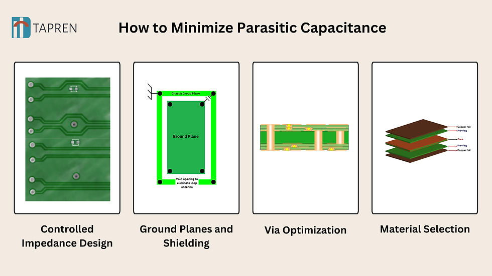
Controlled Impedance Design
A most beneficial aspect is providing uniform width and spacing along the traces to establish a uniform characteristic impedance, thereby minimizing signal reflection. This implies a condition where parasitic capacitive-coupled areas mainly cause the development of emergent impedance mismatches. In these cases, particularly at high speed, differential pairs and transmission lines, controlled impedance becomes even more significant. Early in the design process, utilizing simulation tools will go a long way in achieving credible accuracy in impedance control.
Ground Planes and Shielding
Separated point ground planes will provide a stable reference point around which the signal traces can spread and compensate for this coupling as much as possible through cable isolation, even with their use. A ground plane will suffice for that, as it acts as a shield against EMI and noise coupling. Stacking high-speed signals between ground planes (stripline configuration) additionally improves isolation and lowers parasitic capacitance.
Via Optimization
Wherever possible, the fewest possible vias should be present in paths traversed by high-speed signals, thereby reducing capacitive loading and impedance discontinuities. Also, each time vias must be present, audience placement and continuity of the return path ensure the integrity of the signal measured by the reception. Back-drilling techniques for eliminating use via stubs also lower parasitic capacitance.
Material Selection
It can also be established that the maximum likely parasitic capacitance is achieved using low relative dielectric PCB materials. Low-dielectric materials will equally brace supplementary electric field coupling between conductors, improving high-speed and RF performance. Advanced materials, such as Roger or PTFE, are suitable for these kinds of RF and high-speed digital designs. Thus, selecting the right material would mean a lot more towards signal integrity, thereby avoiding noise couplings.
These design and layout considerations help reduce parasitic effects, ensuring efficient and reliable high-performance PCB designs.
Simulation Tools and Measurement Techniques
Accurate parasitic capacitance analysis calls for sophisticated simulation and measurement methods:

Ansys HFSS: A 3D electromagnetic simulator that simulates complex structures through the Finite Element Method (FEM). It aids in visualizing electric field interaction and minimizing parasitic capacitance, thus making it suitable for RF and high-speed PCB designs.
Cadence Sigrity: Emphasizes signal and power integrity analysis through precise parasitic capacitance and inductance modeling. It models crosstalk and impedance mismatches, ensuring design compliance at high-speed levels before prototyping.
Keysight ADS: Offers time-domain and frequency-domain analysis of high-speed circuits. It models the effect of parasitic capacitance on signal integrity and combines it with measurement hardware for design validation.
Parasitic capacitance can be properly measured using:

Network Analyzers: Impedance and capacitance measurement across a wide frequency range, which is helpful for detecting parasitic capacitance and impedance mismatch. They compare simulated and actual results.
Time Domain Reflectometry (TDR): Emits a high-speed pulse on a transmission line to sense impedance discontinuities due to parasitic capacitance. Properly diagnose signal reflections, crosstalk, and propagation delays in high-speed PCBs.

These methods and tools enable designers to analyze and reduce parasitic capacitance, leading to enhanced PCB performance.
Related Read: Top 5 PCB Design Mistakes
Prototyping and Testing

Prototyping and testing are crucial in ensuring the validation of the effects of parasitic capacitance on the performance of PCBs:
Prototyping: Physical prototypes confirm design assumptions and simulation outcomes. They offer real-world insight into parasitic effects, allowing designers to make any necessary changes before mass production.
Testing under Actual Operating Conditions: Prototypes are tested under actual operating conditions to check signal integrity, noise coupling, and circuit performance. Thus, functional and reliability requirements are met.
Interactive Iterations: Feedback reveals issues based on parasitic capacitance. Designers make iterative modifications in the layout to optimize a signal path, reduce crosstalk, and match impedance.
Prototyping and testing ensure that the final PCB design operates as intended, reducing parasitic capacitance and enhancing overall reliability.
Conclusion
Parasitic capacitance is a crucial consideration in PCB design, as it can significantly impact signal integrity, impedance matching, and overall circuit performance. The higher the operating frequencies, the greater their influence comes into play, resulting in problems such as crosstalk, signal attenuation, and propagation delays. Because designers understand the origin of parasitic capacitance and its associated parameters, they can effectively devise mitigation mechanisms. These include modifications in trace routing with detailed geometry optimization, controlled impedance design, and material selection. Combined with a suitable measurement technique, advanced simulation software, and rigorous prototyping, high-performance and stable PCB designs are ensured while minimizing parasitic effects.
Tapren, a leader in PCB innovation, leverages advanced solutions to address parasitic capacitance and its impact on circuit performance. With Tapren's expertise, you can optimize your PCB designs to ensure signal integrity and minimize delays. By incorporating our strategies and various PCB-related services, you can minimize unwanted capacitance, streamline your design process, and prevent future costly issues.
Key Takeaways
Parasitic capacitance originates from unintended capacitive coupling between conductors on a PCB.
Major techniques for reducing these effects include optimal trace routing, controlled impedance design, and proper material selection.
Simulation tools and measurement methods are very important for accurate analysis and verification.
Validation through prototyping and testing ensures reliable performance.


Comments